- 您现在的位置:买卖IC网 > PDF目录30750 > LM3876MDC (NATIONAL SEMICONDUCTOR CORP) 56 W, 1 CHANNEL, AUDIO AMPLIFIER, UUC PDF资料下载
参数资料
| 型号: | LM3876MDC |
| 厂商: | NATIONAL SEMICONDUCTOR CORP |
| 元件分类: | 音频/视频放大 |
| 英文描述: | 56 W, 1 CHANNEL, AUDIO AMPLIFIER, UUC |
| 封装: | DIE |
| 文件页数: | 16/22页 |
| 文件大小: | 613K |
| 代理商: | LM3876MDC |
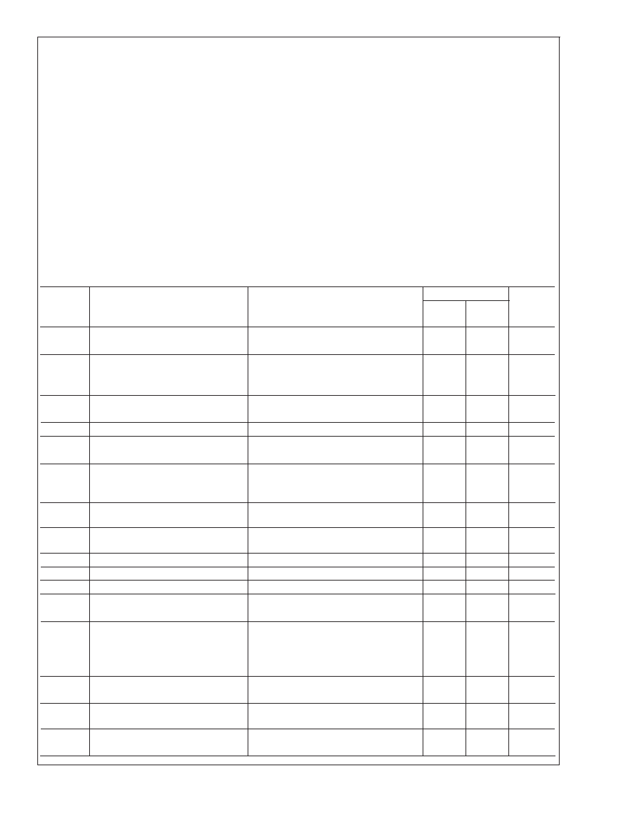
Absolute Maximum Ratings (Notes 4, 5)
If Military/Aerospace specified devices are required,
please contact the National Semiconductor Sales Office/
Distributors for availability and specifications.
Supply Voltage |V
+|+|V| (No Signal)
94V
Supply Voltage |V
+|+|V| (Input Signal)
84V
Common Mode Input Voltage
(V
+ or V) and
|V
+|+|V|
≤80V
Differential Input Voltage
60V
Output Current
Internally Limited
Power Dissipation (Note 6)
125W
ESD Susceptibility (Note 7)
3000V
Junction Temperature (Note 8)
150C
Soldering Information
T Package (10 seconds)
260C
Storage Temperature
40C to +150C
Thermal Resistance
θ
JC
1C/W
θ
JA
43C/W
Operating Ratings (Notes 4, 5)
Temperature Range
T
MIN ≤ TA ≤ TMAX
20C
≤ T
A ≤ +85C
Supply Voltage |V
+|+|V|
24V to 84V
Note 1: Operation is guaranteed up to 84V, however, distortion may be intro-
duced from SPiKe Protection Circuitry when operating above 70V if proper
thermal considerations are not taken into account. Refer to the Thermal
Considerations section for more information.
(See SPiKe Protection Response)
Electrical Characteristics (Notes 4, 5)
The following specifications apply for V
+ = +35V, V = 35V, I
MUTE = 0.5 mA with RL =8 unless otherwise specified. Limits
apply for T
A = 25C.
Symbol
Parameter
Conditions
LM3876
Units
(Limits)
Typical
Limit
(Note 9) (Note 10)
|V
+|+|V|
Power Supply Voltage (Note 13)
V
pin7 V
≥ 9V
18
24
V (min)
84
V (max)
A
M
Mute Attenuation
Pin 8 Open or at 0V, Mute: On
Current out of Pin 8 > 0.5 mA,
120
80
dB (min)
Mute: Off
P
O
(Note 3)
Output Power (Continuous Average)
THD + N = 0.1% (max)
56
40
W (min)
f = 1 kHz; f = 20 kHz
Peak P
O
Instantaneous Peak Output Power
100
W
THD + N
Total Harmonic Distortion Plus Noise
40W, 20 Hz
≤ f ≤ 20 kHz
0.06
%
A
V =26 dB
SR
(Note 3)
Slew Rate (Note 12)
V
IN = 1.2 Vrms, f = 10 kHz,
11
5
V/s
(min)
Square-Wave, R
L =2 k
I
+ (Note 2)
Total Quiescent Power Supply
Current
V
CM = 0V, Vo = 0V, Io = 0A, Imute = 0A
30
70
mA (max)
V
OS
(Note 2)
Input Offset Voltage
V
CM = 0V, Io = 0 mA
1
15
mV (max)
I
B
Input Bias Current
V
CM = 0V, Io = 0 mA
0.2
1
A (max)
I
OS
Input Offset Current
V
CM = 0V, Io = 0 mA
0.01
0.2
A (max)
I
o
Output Current Limit
|V
+|=|V| = 12V, t
ON = 10 ms, VO = 0V
6
4
A (min)
V
od
(Note 2)
Output Dropout Voltage (Note 14)
|V
+–V
O|, V
+ = 20V, I
o = +100 mA
1.6
5
V (max)
|V
O–V
|, V = 20V, I
o = 100 mA
2.7
5
V (max)
PSRR
(Note 2)
Power Supply Rejection Ratio
V
+ = 40V to 20V, V = 40V,
120
85
dB (min)
V
CM = 0V, Io =0 mA
V
+ = 40V, V = 40V to 20V,
120
85
dB (min)
V
CM = 0V, Io =0 mA
CMRR
(Note 2)
Common Mode Rejection Ratio
V
+ = 60V to 20V, V = 20V to 60V,
120
80
dB (min)
V
CM = 20V to 20V, Io =0 mA
A
VOL
(Note 2)
Open Loop Voltage Gain
|V
+|=|V| = 40V, R
L =2 k, VO = 60V
120
90
dB (min)
GBWP
Gain-Bandwidth Product
|V
+|=|V| = 40V
8
2
MHz
(min)
f
O = 100 kHz, VIN = 50 mVrms
LM3876
www.national.com
3
相关PDF资料 |
PDF描述 |
|---|---|
| LM387N | VIDEO PREAMPLIFIER, PDIP8 |
| LM387V | 2 CHANNEL, VIDEO PREAMPLIFIER, PDIP8 |
| LM3886DWF | 68 W, 1 CHANNEL, AUDIO AMPLIFIER, UUC |
| LM3886MWC | 68 W, 1 CHANNEL, AUDIO AMPLIFIER, UUC |
| LM3909N | SPECIALTY CONSUMER CIRCUIT, PDIP8 |
相关代理商/技术参数 |
参数描述 |
|---|---|
| LM3876T | 功能描述:音频放大器 RoHS:否 制造商:STMicroelectronics 产品:General Purpose Audio Amplifiers 输出类型:Digital 输出功率: THD + 噪声: 工作电源电压:3.3 V 电源电流: 最大功率耗散: 最大工作温度: 安装风格:SMD/SMT 封装 / 箱体:TQFP-64 封装:Reel |
| LM3876T | 制造商:National Semiconductor Corporation 功能描述:56W W/Mute, 1 Channel Lm3876T IC Audio Amp |
| LM3876T/NOPB | 功能描述:音频放大器 RoHS:否 制造商:STMicroelectronics 产品:General Purpose Audio Amplifiers 输出类型:Digital 输出功率: THD + 噪声: 工作电源电压:3.3 V 电源电流: 最大功率耗散: 最大工作温度: 安装风格:SMD/SMT 封装 / 箱体:TQFP-64 封装:Reel |
| LM3876TF | 功能描述:音频放大器 RoHS:否 制造商:STMicroelectronics 产品:General Purpose Audio Amplifiers 输出类型:Digital 输出功率: THD + 噪声: 工作电源电压:3.3 V 电源电流: 最大功率耗散: 最大工作温度: 安装风格:SMD/SMT 封装 / 箱体:TQFP-64 封装:Reel |
| LM3876TF NOPB | 制造商:Texas Instruments 功能描述:8MHz Class-AB Bulk |
发布紧急采购,3分钟左右您将得到回复。