- 您现在的位置:买卖IC网 > PDF目录240278 > LM4041DIM3-ADJT&R (MICREL INC) 1-OUTPUT TWO TERM VOLTAGE REFERENCE, 1.233 V, PDSO3 PDF资料下载
参数资料
| 型号: | LM4041DIM3-ADJT&R |
| 厂商: | MICREL INC |
| 元件分类: | 基准电压源/电流源 |
| 英文描述: | 1-OUTPUT TWO TERM VOLTAGE REFERENCE, 1.233 V, PDSO3 |
| 封装: | SOT-23, 3 PIN |
| 文件页数: | 2/16页 |
| 文件大小: | 812K |
| 代理商: | LM4041DIM3-ADJT&R |
LM4040/4041
Micrel, Inc.
M9999-031805
10
March 2005
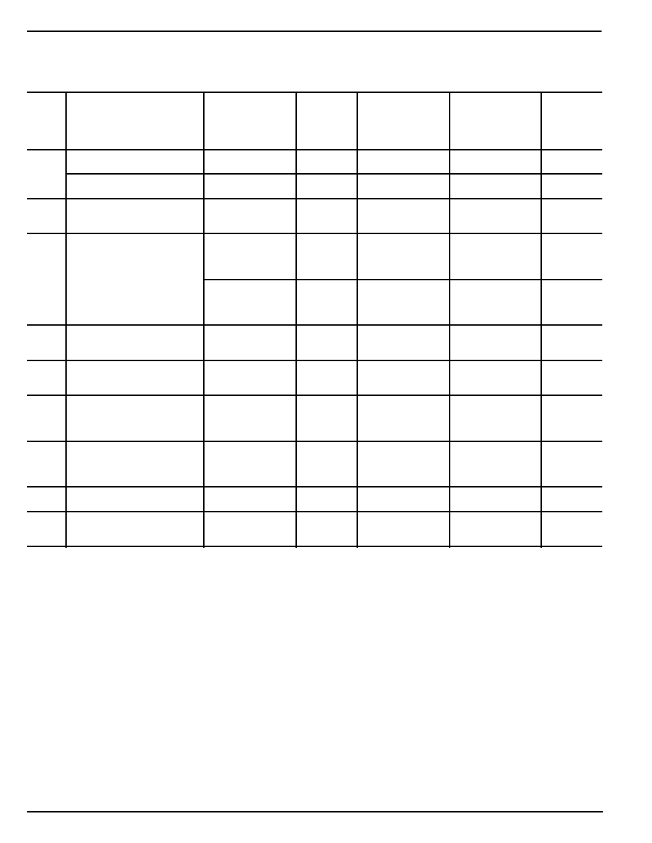
LM4041-Adjustable Electrical Characteristics (Note 4)
Boldface limits apply for TA = TJ = TMIN to TMAX; all other limits TJ = 25°C unless otherwise specied (SOT-23, see Note 8),
IRMIN ≤ IR < 12mA, VREF ≤ VOUT ≤ 10V. The grades C and D designate initial Reverse Breakdown Voltage tolerance of ±0.5% and ±1%,
respectively for VOUT = 5V.
LM4041CIM3
LM4041DIM3
Symbol
Parameter
Conditions
Typical
Units
(Note 5)
Limits
(Limit)
(Note 6)
VREF
Reference Breakdown Voltage
IR = 100A
1.233
V
VOUT = 5V
Reference Breakdown Voltage
IR = 100A
±6.2
±12
mV (max)
Tolerance
(Note 9)
±14
±24
mV (max)
IRMIN
Minimum Operating Current
45
A
60
65
A (max)
65
70
A (max)
ΔVREF
Reference Voltage
IRMIN ≤ IR 1mA
0.7
mV
/ΔIR
Change with Operating
SOT-23:
1.5
2.0
mV (max)
Current Change
VOUT ≥ 1.6V
2.0
2.5
mV (max)
(Note 8)
1mA ≤ IR 15mA
2
mV
SOT-23:
4
6
mV (max)
VOUT ≥ 1.6V
6
8
mV (max)
(Note 8)
ΔVREF
Reference Voltage Change
IR = 1mA
–1.55
mV/V
/ΔVO
with Output Voltage Change
–2.0
–2.5
mV/V (max)
–2.5
–3.0
mV/V (max)
IFB
Feedback Current
60
nA
100
150
nA (max)
120
200
nA (max)
ΔVREF
Average Reference
VOUT = 5V
/ΔT
Voltage Temperature
IR = 10mA
±20
ppm/°C
Coefcient
IR = 1mA
±15
±100
±150
ppm/°C (max)
(Note 9)
IR = 100A
±15
ppm/°C (max)
ZOUT
Dynamic Output Impedance
IR = 1mA, f = 120Hz
IAC = 0.1 IR
VOUT = VREF
0.3
Ω
VOUT = 10V
2
Ω (max)
eN
Wideband Noise
IR = 100A
10Hz ≤ f ≤ 10kHz
20
VRMS
ΔVREF
Reference Voltage
t = 1000hrs
Long Term Stability
T = 25°C ±0.1°C
120
ppm
IR = 100A
Note 4. Specication for packaged product only.
Note 5. Typicals are at TJ = 25°C and represent most likely parametric norm.
Note 6. Limits are 100% production tested at 25°C. Limits over temperature are guaranteed through correlation using Statistical Quality Control (SQL)
methods.
Note 7. The boldface (over temperature limit for Reverse Breakdown Voltage Tolerance is dened as the room temperature Reverse Breakdown Volt-
age Tolerance ±[(ΔVR/ΔT)(65°C)(VR)]. ΔVR/ΔT is the VR temperature coefcient, 65°C is the temperature range from –40°C to the reference
point of 25°C, and VR is the reverse breakdown voltage. The total over temperature tolerance for the different grades follows:
C-grade: ±1.15% = ±0.5% ±100ppm/°C × 65°C
D-grade: ±1.98% = ±1.0% ±150ppm/°C × 65°C
Example: The C-grade LM4040-2.5 has an over temperature Reverse Breakdown Voltage tolerance of ±2.5 × 1.15% = ±29mV.
Note 8. When VOUT ≤ 1.6V, the LM4041-ADJ must operate at reduced IR. This is caused by the series resistance of the die attach between the die (–)
output and the package (–) output pin. See the Output Saturation curve in the “Typical Performance Characteristics” section.
Note 9. Reference voltage and temperature coefcient will change with output voltage. See “Typical Performance Characteristics” curves.
相关PDF资料 |
PDF描述 |
|---|---|
| LS4301-9PD8TB1 | 1-OUTPUT 100 W AC-DC PWR FACTOR CORR MODULE |
| LS4501-9PD4TB1 | 1-OUTPUT 100 W AC-DC PWR FACTOR CORR MODULE |
| LS4501-9PD9TB1 | 1-OUTPUT 100 W AC-DC PWR FACTOR CORR MODULE |
| LKP5660-5EPDDTB1 | 2-OUTPUT 250 W AC-DC PWR FACTOR CORR MODULE |
| LPC1902-7D | 1-OUTPUT 230 W AC-DC PWR FACTOR CORR MODULE |
相关代理商/技术参数 |
参数描述 |
|---|---|
| LM4041DIM3-ADJTR | 制造商:Rochester Electronics LLC 功能描述:- Tape and Reel |
| LM4041DIM3X-1.2 | 功能描述:基准电压& 基准电流 RoHS:否 制造商:STMicroelectronics 产品:Voltage References 拓扑结构:Shunt References 参考类型:Programmable 输出电压:1.24 V to 18 V 初始准确度:0.25 % 平均温度系数(典型值):100 PPM / C 串联 VREF - 输入电压(最大值): 串联 VREF - 输入电压(最小值): 分流电流(最大值):60 mA 最大工作温度:+ 125 C 封装 / 箱体:SOT-23-3L 封装:Reel |
| LM4041DIM3X-1.2/NOPB | 功能描述:基准电压& 基准电流 RoHS:否 制造商:STMicroelectronics 产品:Voltage References 拓扑结构:Shunt References 参考类型:Programmable 输出电压:1.24 V to 18 V 初始准确度:0.25 % 平均温度系数(典型值):100 PPM / C 串联 VREF - 输入电压(最大值): 串联 VREF - 输入电压(最小值): 分流电流(最大值):60 mA 最大工作温度:+ 125 C 封装 / 箱体:SOT-23-3L 封装:Reel |
| LM4041DIM3X12 | 制造商:NATIONAL 功能描述:* |
| LM4041DIM3XADJ | 制造商:NATIONAL 功能描述:New |
发布紧急采购,3分钟左右您将得到回复。