- 您现在的位置:买卖IC网 > PDF目录17480 > LM4050CEM3-5.0+T (Maxim Integrated Products)IC VREF SHUNT PREC 5V SOT-23-3 PDF资料下载
参数资料
| 型号: | LM4050CEM3-5.0+T |
| 厂商: | Maxim Integrated Products |
| 文件页数: | 11/14页 |
| 文件大小: | 0K |
| 描述: | IC VREF SHUNT PREC 5V SOT-23-3 |
| 产品培训模块: | Lead (SnPb) Finish for COTS Obsolescence Mitigation Program |
| 标准包装: | 1 |
| 基准类型: | 旁路,精度 |
| 输出电压: | 5V |
| 容差: | ±0.5% |
| 温度系数: | 50ppm/°C |
| 通道数: | 1 |
| 电流 - 阴极: | 80µA |
| 电流 - 输出: | 15mA |
| 工作温度: | -40°C ~ 125°C |
| 安装类型: | 表面贴装 |
| 封装/外壳: | TO-236-3,SC-59,SOT-23-3 |
| 供应商设备封装: | SOT-23-3 |
| 包装: | 标准包装 |
| 产品目录页面: | 1426 (CN2011-ZH PDF) |
| 其它名称: | LM4050CEM3-5.0+TDKR |
�� �
�
�LM4050/LM4051�
�50ppm/°C� Precision� Micropower� Shunt� Voltage�
�References� with� Multiple� Reverse� Breakdown� Voltages�
�Pin� Description�
�PIN�
�1�
�2�
�3�
�NAME�
�+�
�?�
�N.C.�
�FUNCTION�
�Positive� Terminal� of� the� Shunt� Reference�
�Negative� Terminal� of� the� Shunt� Reference�
�No� connection.� Leave� this� pin� unconnected� or� connected� to� pin� 2.�
�Detailed� Description�
�The� LM4050/LM4051� shunt� references� use� the�
�bandgap� principle� to� produce� a� stable,� accurate� volt-�
�age.� The� device� behaves� similarly� to� an� ideal� zener�
�diode;� a� fixed� voltage� is� maintained� across� its� output�
�terminals� when� biased� with� 60μA� to� 15mA� of� reverse�
�current.� The� LM4050/LM4051� clamps� to� a� voltage� of�
�one� diode� drop� below� ground� when� biased� with� for-�
�ward� currents� up� 10mA.�
�Figure� 3� shows� a� typical� operating� circuit.� The�
�LM4050/LM4051� are� ideal� for� providing� stable� refer-�
�ences� from� a� high-voltage� power� supply.�
�Applications� Information�
�The� LM4050/LM4051s’� internal� pass� transistors� are� used�
�to� maintain� a� constant� output� voltage� (V� SHUNT� )� by� sinking�
�the� necessary� amount� of� current� across� a� source� resistor.�
�The� source� resistance� (R� S� )� is� determined� from� the� load�
�current� (I� LOAD� )� range,� supply� voltage� (V� S� )� variations,�
�V� SHUNT� ,� and� desired� quiescent� current.�
�Choose� the� value� of� R� S� when� V� S� is� at� a� minimum� and� I� LOAD�
�is� at� a� maximum.� Maintain� a� minimum� I� SHUNT� of� 60μA� at� all�
�times.� The� R� S� value� should� be� large� enough� to� keep�
�I� SHUNT� less� than� 15mA� for� proper� regulation� when� V� S� is�
�maximum� and� I� LOAD� is� at� a� minimum.� To� prevent� damage�
�to� the� device,� I� SHUNT� should� never� exceed� 20mA.�
�Therefore,� the� value� of� R� S� is� bounded� by� the� following�
�equation:�
�[V� S(MIN)� -� V� R� ]� /� [60μA� +� I� LOAD(MAX)� ]� >� R� S� >�
�[V� S(MAX)� -� V� R� ]� /� [20mA� +� I� LOAD(MIN)� ]�
�Choosing� a� larger� resistance� minimizes� the� total� power� dis-�
�sipation� in� the� circuit� by� reducing� the� shunt� current�
�(P� D(TOTAL)� =� V� S� � I� SHUNT� ).� Provide� a� safety� margin� to�
�incorporate� the� worst-case� tolerance� of� the� resistor� used.�
�Ensure� that� the� resistor’s� power� rating� is� adequate,� using�
�the� following� general� power� equation:�
�PD� R� =� I� SHUNT� � (V� S(MAX)� -� V� SHUNT� )�
�Output� Capacitance�
�The� LM4050/LM4051� do� not� require� external� capacitors�
�for� frequency� stability� and� are� stable� for� any� output�
�capacitance.�
�Maxim� Integrated�
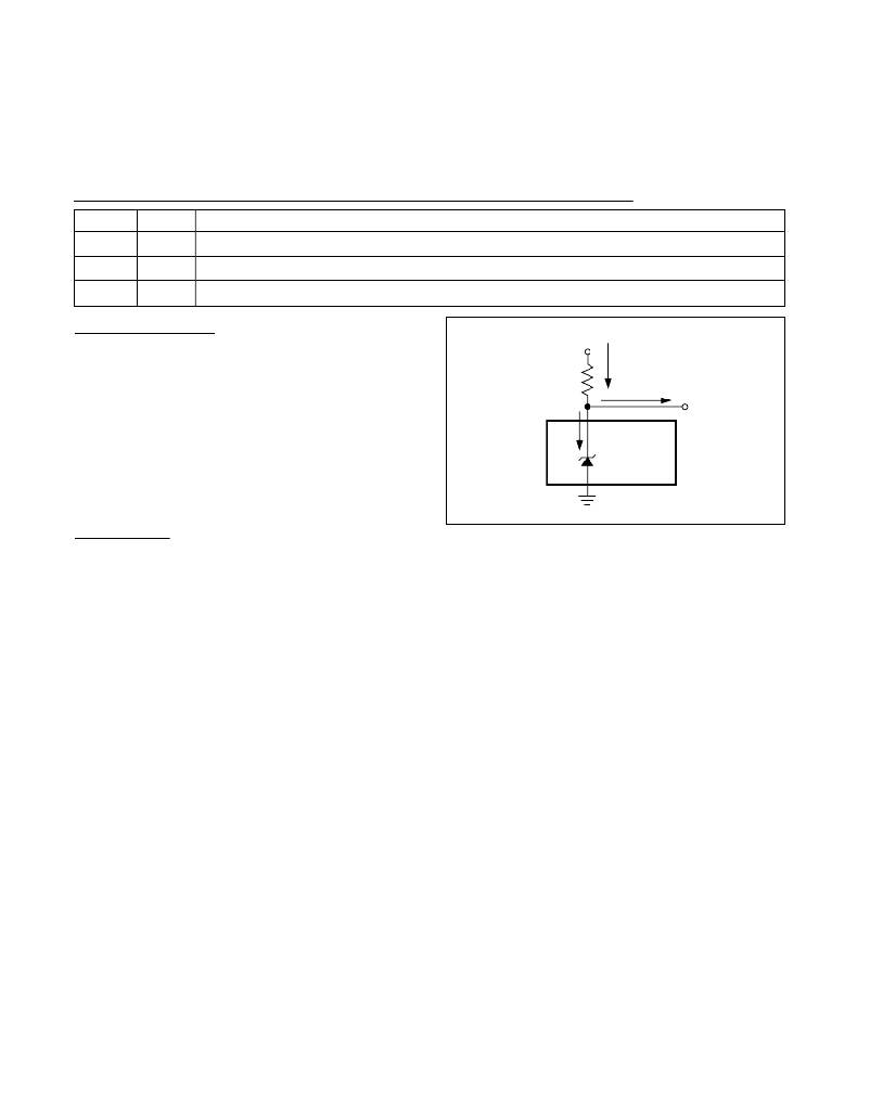
�V� S�
�I� SHUNT� +� I� LOAD�
�R� S�
�I� LOAD�
�V� R�
�I� SHUNT�
�LM4050�
�Figure� 3.� Typical� Operating� Circuit�
�Temperature� Performance�
�The� LM4050/LM4051� typically� exhibit� output� voltage�
�temperature� coefficients� within� ±15ppm/°C.� The� polari-�
�ty� of� the� temperature� coefficients� may� be� different� from�
�one� device� to� another;� some� may� have� positive� coeffi-�
�cients,� and� others� may� have� negative� coefficients.�
�High� Temperature� Operation�
�The� maximum� junction� temperature� of� the� LM4050/�
�LM4051� is� +150°C.� The� maximum� operating� temperature�
�for� the� LM4050/LM4051_E_� is� +125°C.� At� a� maximum�
�load� current� of� 15mA� and� a� maximum� output� voltage� of�
�5V,� the� parts� dissipate� 75mW� of� power.� The� power� dissi-�
�pation� limits� of� the� 3-pin� SC70� call� for� a� derating� value� of�
�2.17mW/°C� above� +70°C� and� thus� for� 75mW� of� power�
�dissipation,� the� parts� self-heat� to� 35.56°C� above� ambient�
�temperature.� If� the� ambient� temperature� is� +125°C,� the�
�parts� operate� at� 159.56°C,� thereby� exceeding� the� maxi-�
�mum� junction� temperature� value� of� +150°C.� For� high-�
�temperature� operation,� care� must� be� taken� to� ensure� the�
�combination� of� ambient� temperature,� output� power� dissi-�
�pation,� and� package� thermal� resistance� does� not� con-�
�spire� to� raise� the� device� temperature� beyond� that� listed�
�in� the� Absolute� Maximum� Ratings.� Either� reduce� the� out-�
�put� load� current� or� the� ambient� temperature� to� keep� the�
�part� within� the� limits.�
�11�
�相关PDF资料 |
PDF描述 |
|---|---|
| PV32T250A02B00 | TRIMMER 25 OHM 0.5W TH |
| PV32T205A02B00 | TRIMMER 2M OHM 0.5W TH |
| PV32T204A02B00 | TRIMMER 200K OHM 0.5W TH |
| PV32T203A02B00 | TRIMMER 20K OHM 0.5W TH |
| S2M/54 | RECTIFIER 1000V 1.5A SMB |
相关代理商/技术参数 |
参数描述 |
|---|---|
| LM4050CEM3-8.2/NOPB | 功能描述:IC VREF SHUNT PREC 8.192V SOT23 RoHS:是 类别:集成电路 (IC) >> PMIC - 电压基准 系列:- 标准包装:1 系列:- 基准类型:串联,精度 输出电压:4.5V 容差:±800µV 温度系数:1ppm/°C 输入电压:13.5 V ~ 22 V 通道数:1 电流 - 阴极:- 电流 - 静态:7mA 电流 - 输出:10mA 工作温度:-55°C ~ 125°C 安装类型:表面贴装 封装/外壳:20-LCC 供应商设备封装:20-CLCC 包装:管件 |
| LM4050CEM3X-10/NOPB | 功能描述:IC VREF SHUNT PREC 10V SOT-23-3 RoHS:是 类别:集成电路 (IC) >> PMIC - 电压基准 系列:- 标准包装:3,000 系列:- 基准类型:旁路,精度 输出电压:5V 容差:±0.5% 温度系数:100ppm/°C 输入电压:- 通道数:1 电流 - 阴极:80µA 电流 - 静态:- 电流 - 输出:15mA 工作温度:-40°C ~ 85°C 安装类型:表面贴装 封装/外壳:TO-236-3,SC-59,SOT-23-3 供应商设备封装:SOT-23-3 包装:带卷 (TR) 其它名称:LM4040CIM3-5.0MLTRLM4040CIM3-5.0MLTR-ND |
| LM4050CEM3X-2.0/NOPB | 功能描述:IC VREF SHUNT PREC 2.048V SOT23 RoHS:是 类别:集成电路 (IC) >> PMIC - 电压基准 系列:- 标准包装:3,000 系列:- 基准类型:旁路,精度 输出电压:5V 容差:±0.5% 温度系数:100ppm/°C 输入电压:- 通道数:1 电流 - 阴极:80µA 电流 - 静态:- 电流 - 输出:15mA 工作温度:-40°C ~ 85°C 安装类型:表面贴装 封装/外壳:TO-236-3,SC-59,SOT-23-3 供应商设备封装:SOT-23-3 包装:带卷 (TR) 其它名称:LM4040CIM3-5.0MLTRLM4040CIM3-5.0MLTR-ND |
| LM4050CEM3X-2.5 | 功能描述:基准电压& 基准电流 RoHS:否 制造商:STMicroelectronics 产品:Voltage References 拓扑结构:Shunt References 参考类型:Programmable 输出电压:1.24 V to 18 V 初始准确度:0.25 % 平均温度系数(典型值):100 PPM / C 串联 VREF - 输入电压(最大值): 串联 VREF - 输入电压(最小值): 分流电流(最大值):60 mA 最大工作温度:+ 125 C 封装 / 箱体:SOT-23-3L 封装:Reel |
| LM4050CEM3X-2.5/NOPB | 功能描述:基准电压& 基准电流 RoHS:否 制造商:STMicroelectronics 产品:Voltage References 拓扑结构:Shunt References 参考类型:Programmable 输出电压:1.24 V to 18 V 初始准确度:0.25 % 平均温度系数(典型值):100 PPM / C 串联 VREF - 输入电压(最大值): 串联 VREF - 输入电压(最小值): 分流电流(最大值):60 mA 最大工作温度:+ 125 C 封装 / 箱体:SOT-23-3L 封装:Reel |
发布紧急采购,3分钟左右您将得到回复。