- 您现在的位置:买卖IC网 > PDF目录30752 > LM4810LD/NOPB (NATIONAL SEMICONDUCTOR CORP) 0.105 W, 2 CHANNEL, AUDIO AMPLIFIER, DSO8 PDF资料下载
参数资料
| 型号: | LM4810LD/NOPB |
| 厂商: | NATIONAL SEMICONDUCTOR CORP |
| 元件分类: | 音频/视频放大 |
| 英文描述: | 0.105 W, 2 CHANNEL, AUDIO AMPLIFIER, DSO8 |
| 封装: | LLP-8 |
| 文件页数: | 5/18页 |
| 文件大小: | 928K |
| 代理商: | LM4810LD/NOPB |
Application Information (Continued)
the magnitude of “clicks and pops”. Increasing the value of
C
B reduces the magnitude of turn-on pops. However, this
presents a tradeoff: as the size of C
B increases, the turn-on
time increases. There is a linear relationship between the
size of C
B and the turn-on time. Here are some typical
turn-on times for various values of C
B:
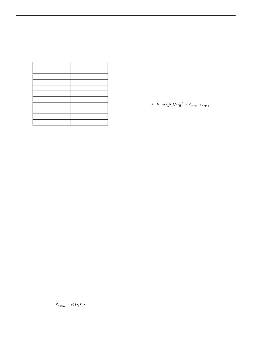
C
B
T
ON
0.1F
80ms
0.22F
170ms
0.33F
270ms
0.47F
370ms
0.68F
490ms
1.0F
920ms
2.2F
1.8sec
3.3F
2.8sec
4.7F
3.4sec
10F
7.7sec
In order eliminate “clicks and pops”, all capacitors must be
discharged before turn-on. Rapidly switching V
DD may not
allow the capacitors to fully discharge, which may cause
“clicks and pops”. In a single-ended configuration, the output
is coupled to the load by C
O. This capacitor usually has a
high value. C
O discharges through internal 20k
resistors.
Depending on the size of C
O, the discharge time constant
can be relatively large. To reduce transients in single-ended
mode, an external 1k
–5k resistor can be placed in par-
allel with the internal 20k
resistor. The tradeoff for using
this resistor is increased quiescent current.
AUDIO POWER AMPLIFIER DESIGN
Design a Dual 70mW/32
Audio Amplifier
Given:
Power Output
70 mW
Load Impedance
32
Input Level
1 Vrms (max)
Input Impedance
20k
Bandwidth
100 Hz–20 kHz ± 0.50dB
The design begins by specifying the minimum supply voltage
necessary to obtain the specified output power. One way to
find the minimum supply voltage is to use the Output Power
vs Supply Voltage curve in the Typical Performance Char-
acteristics section. Another way, using Equation (5), is to
calculate the peak output voltage necessary to achieve the
desired output power for a given load impedance. To ac-
count for the amplifier’s dropout voltage, two additional volt-
ages, based on the Dropout Voltage vs Supply Voltage in the
Typical Performance Characteristics curves, must be
added to the result obtained by Equation (5). For a
single-ended application, the result is Equation (6).
(5)
V
DD
≥ (2V
OPEAK +(VODTOP +VODBOT))
(6)
The Output Power vs Supply Voltage graph for a 32
load
indicates a minimum supply voltage of 4.8V. This is easily
met by the commonly used 5V supply voltage. The additional
voltage creates the benefit of headroom, allowing the
LM4810 to produce peak output power in excess of 70mW
without clipping or other audible distortion. The choice of
supply voltage must also not create a situation that violates
maximum power dissipation as explained above in the
Power Dissipation section. Remember that the maximum
power dissipation point from Equation (1) must be multiplied
by two since there are two independent amplifiers inside the
package. Once the power dissipation equations have been
addressed, the required gain can be determined from Equa-
tion (7).
(7)
Thus, a minimum gain of 1.497 allows the LM4810 to reach
full output swing and maintain low noise and THD+N perfro-
mance. For this example, let A
V=1.5.
The amplifiers overall gain is set using the input (R
i ) and
feedback (R
f ) resistors. With the desired input impedance
set at 20k
, the feedback resistor is found using Equation
(8).
A
V =Rf/Ri
(8)
The value of R
f is 30k
.
The last step in this design is setting the amplifier’s 3db
frequency bandwidth. To achieve the desired ±0.25dB pass
band magnitude variation limit, the low frequency response
must extend to at lease onefifth the lower bandwidth limit
and the high frequency response must extend to at least five
times the upper bandwidth limit. The gain variation for both
response limits is 0.17dB, well within the ±0.25dB desired
limit. The results are an
f
L = 100Hz/5 = 20Hz
(9)
and a
f
H = 20kHz
*
5 = 100kHz
(10)
As stated in the External Components section, both R
i in
conjunction with C
i, and Co with RL, create first order high-
pass filters. Thus to obtain the desired low frequency re-
sponse of 100Hz within ±0.5dB, both poles must be taken
into consideration. The combination of two single order filters
at the same frequency forms a second order response. This
results in a signal which is down 0.34dB at five times away
from the single order filter 3dB point. Thus, a frequency of
20Hz is used in the following equations to ensure that the
response is better than 0.5dB down at 100Hz.
C
i
≥ 1/(2π * 20k * 20Hz) = 0.397F; use 0.39F.(11)
C
o
≥ 1/(2π *32 * 20Hz) = 249F; use 330F. (12)
The high frequency pole is determined by the product of the
desired high frequency pole, f
H, and the closed-loop gain,
LM4810
www.national.com
13
相关PDF资料 |
PDF描述 |
|---|---|
| LM4810M | 0.105 W, 2 CHANNEL, AUDIO AMPLIFIER, PDSO8 |
| LM4816MT/NOPB | 1.5 W, 2 CHANNEL, AUDIO AMPLIFIER, PDSO20 |
| LM4817MH/NOPB | 1.5 W, 2 CHANNEL, AUDIO AMPLIFIER, PDSO28 |
| LM4818M/NOPB | 0.35 W, 1 CHANNEL, AUDIO AMPLIFIER, PDSO8 |
| LM4820MMX-6 | 1 W, 1 CHANNEL, AUDIO AMPLIFIER, PDSO8 |
相关代理商/技术参数 |
参数描述 |
|---|---|
| LM4810MA | 制造商:NSC 制造商全称:National Semiconductor 功能描述:Dual 105mW Headphone Amplifier with Active-High Shutdown Mode |
| LM4810MA/NOPB | 功能描述:IC AMP AUDIO PWR .105W AB 8SOIC RoHS:是 类别:集成电路 (IC) >> 线性 - 音頻放大器 系列:Boomer® 产品培训模块:Lead (SnPb) Finish for COTS Obsolescence Mitigation Program 标准包装:2,500 系列:DirectDrive® 类型:H 类 输出类型:耳机,2-通道(立体声) 在某负载时最大输出功率 x 通道数量:35mW x 2 @ 16 欧姆 电源电压:1.62 V ~ 1.98 V 特点:I²C,麦克风,静音,短路保护,音量控制 安装类型:表面贴装 供应商设备封装:25-WLP(2.09x2.09) 封装/外壳:25-WFBGA,WLCSP 包装:带卷 (TR) |
| LM4810MM | 制造商:NSC 制造商全称:National Semiconductor 功能描述:Dual 105mW Headphone Amplifier with Active-High Shutdown Mode |
| LM4810MM/NOPB | 功能描述:音频放大器 LM4810 Dual 105mW Headphone Amp RoHS:否 制造商:STMicroelectronics 产品:General Purpose Audio Amplifiers 输出类型:Digital 输出功率: THD + 噪声: 工作电源电压:3.3 V 电源电流: 最大功率耗散: 最大工作温度: 安装风格:SMD/SMT 封装 / 箱体:TQFP-64 封装:Reel |
| LM4810MMX/NOPB | 功能描述:音频放大器 LM4810 Dual 105mW Headphone Amp RoHS:否 制造商:STMicroelectronics 产品:General Purpose Audio Amplifiers 输出类型:Digital 输出功率: THD + 噪声: 工作电源电压:3.3 V 电源电流: 最大功率耗散: 最大工作温度: 安装风格:SMD/SMT 封装 / 箱体:TQFP-64 封装:Reel |
发布紧急采购,3分钟左右您将得到回复。