- 您现在的位置:买卖IC网 > PDF目录30752 > LM4820IBPX-6/NOPB (NATIONAL SEMICONDUCTOR CORP) 1 W, 1 CHANNEL, AUDIO AMPLIFIER, PBGA8 PDF资料下载
参数资料
| 型号: | LM4820IBPX-6/NOPB |
| 厂商: | NATIONAL SEMICONDUCTOR CORP |
| 元件分类: | 音频/视频放大 |
| 英文描述: | 1 W, 1 CHANNEL, AUDIO AMPLIFIER, PBGA8 |
| 封装: | MICRO, MO-211-BC, SMD-8 |
| 文件页数: | 4/20页 |
| 文件大小: | 994K |
| 代理商: | LM4820IBPX-6/NOPB |
Application Information (Continued)
reproduce signals below 100 Hz to 150 Hz. Thus, using a
large input capacitor may not increase actual system perfor-
mance.
In addition to system cost and size, click and pop perfor-
mance is effected by the size of the input coupling capacitor,
C
i. A larger input coupling capacitor requires more charge to
reach its quiescent DC voltage (nominally 1/2 V
DD). This
charge comes from the output via the feedback and is apt to
create pops upon device enable. Thus, by minimizing the
capacitor size based on necessary low frequency response,
turn-on pops can be minimized.
Besides minimizing the input capacitor size, careful consid-
eration should be paid to the bypass capacitor value. Bypass
capacitor, C
B, is the most critical component to minimize
turn-on pops since it determines how fast the LM4820-6
turns on. The slower the LM4820-6’s outputs ramp to their
quiescent DC voltage (nominally 1/2 V
DD), the smaller the
turn-on pop. Choosing C
B equal to 1.0 F along with a small
value of C
i (in the range of 0.1 F to 0.39 F), should
produce a virtually clickless and popless shutdown function.
While the device will function properly, (no oscillations or
motorboating), with C
B equal to 0.1 F, the device will be
much more susceptible to turn-on clicks and pops. Thus, a
value of C
B equal to 1.0 F is recommended in all but the
most cost sensitive designs.
AUDIO POWER AMPLIFIER DESIGN
A 1W/8
Audio Amplifier
Given:
Power Output
1 Wrms
Load Impedance
8
Input Level
1 Vrms
Input Impedance
25 k
Bandwidth
100 Hz–20 kHz ± 0.25 dB
A designer must first determine the minimum supply rail to
obtain the specified output power. By extrapolating from the
Output Power vs Supply Voltage graphs in the Typical Per-
formance Characteristics section, the supply rail can be
easily found. A second way to determine the minimum sup-
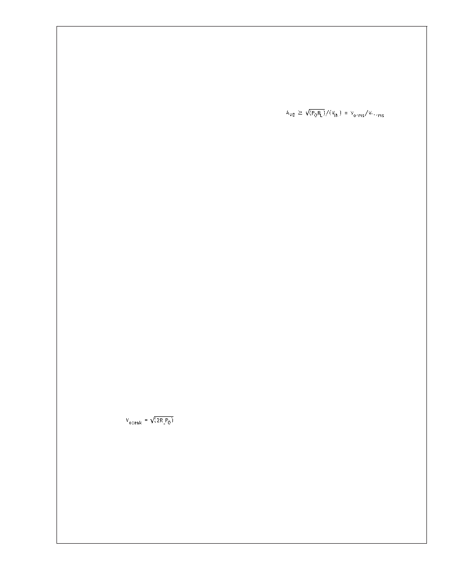
ply rail is to calculate the required V
opeak using Equation 3.
Using this method, the minimum supply voltage would be
(V
opeak +(VODTOP +VODBOT)), where VODBOT and VODTOP are
extrapolated from the Dropout Voltage vs Supply Voltage
curve in the Typical Performance Characteristics section.
(3)
2.7V
DD to 5VDD is a standard supply voltage range for most
applications. Extra supply voltage creates headroom that
allows the LM4820-6 to reproduce peaks in excess of 1W
without producing audible distortion. At this time, the de-
signer must make sure that the power supply choice along
with the output impedance does not violate the conditions
explained in the Power Dissipation section.
Once the power dissipation equations have been addressed,
the differential gain is determined from Equations 4 or 5.
(4)
or
A
VD =2(Rf/Ri )
(5)
R
f =Ri = 25k
A
VD =2(25k
/25k )
A
VD =2
The last step in this design example is setting the amplifier’s
-3dB frequency bandwidth. To achieve the desired ±0.25dB
pass band magnitude variation limit, the low frequency re-
sponse must extend to at least one-fifth the lower bandwidth
limit. The high frequency response must extend to at least
five times the upper bandwidth limit. The gain variation for
both response limits is 0.17dB, well within the ±0.25dB
desired limit. The results are
f
L = 100Hz/5 = 20Hz
and
f
H = 20kHzx5= 100kHz
As mentioned in the Selecting Proper External Compo-
nents section, R
i and Ci create a highpass filter that sets the
amplifier’s lower bandpass frequency limit. To find the cou-
pling capacitor’s value, use Equation 6
C
i
≥ 1/(2πR
ifL)
(6)
The result is
1/(2
π*25k*20kHz) = .318f
Use a 0.33f capacitor, the closest standard value.
The product of the desired high frequency cutoff (100kHz in
this example ) and the differential gain A
VD, determines the
upper passband response limit. With A
VD = 2 and fH =
100kHz, the closed-loop gain bandwidth product (GBWP) is
200kHz. This is less than the LM4820-6’s 25MHz GBWP.
With this margin, the amplifier can be used in designs that
require more differential gain while avoiding performance,
restricting bandwidth limitations.
LM4820-6
www.national.com
12
相关PDF资料 |
PDF描述 |
|---|---|
| LM4830MX | 2 W, 2 CHANNEL, AUDIO AMPLIFIER, PDSO24 |
| LM4831VFX | SPECIALTY CONSUMER CIRCUIT, PQFP44 |
| LM4832M/NOPB | 2 CHANNEL(S), TONE CONTROL CIRCUIT, PDSO28 |
| LM4832MT/NOPB | 2 CHANNEL(S), TONE CONTROL CIRCUIT, PDSO28 |
| LM4834MDC | 2 CHANNEL(S), VOLUME CONTROL CIRCUIT, UUC |
相关代理商/技术参数 |
参数描述 |
|---|---|
| LM4820ITP-6/NOPB | 功能描述:IC AMP AUDIO PWR 1W MONO 8USMD RoHS:是 类别:集成电路 (IC) >> 线性 - 音頻放大器 系列:Boomer® 产品培训模块:Lead (SnPb) Finish for COTS Obsolescence Mitigation Program 标准包装:2,500 系列:DirectDrive® 类型:H 类 输出类型:耳机,2-通道(立体声) 在某负载时最大输出功率 x 通道数量:35mW x 2 @ 16 欧姆 电源电压:1.62 V ~ 1.98 V 特点:I²C,麦克风,静音,短路保护,音量控制 安装类型:表面贴装 供应商设备封装:25-WLP(2.09x2.09) 封装/外壳:25-WFBGA,WLCSP 包装:带卷 (TR) |
| LM4820M-6 | 功能描述:IC AMP AUDIO PWR 1W MONO 8SOIC RoHS:否 类别:集成电路 (IC) >> 线性 - 音頻放大器 系列:Boomer® 产品培训模块:Lead (SnPb) Finish for COTS Obsolescence Mitigation Program 标准包装:2,500 系列:DirectDrive® 类型:H 类 输出类型:耳机,2-通道(立体声) 在某负载时最大输出功率 x 通道数量:35mW x 2 @ 16 欧姆 电源电压:1.62 V ~ 1.98 V 特点:I²C,麦克风,静音,短路保护,音量控制 安装类型:表面贴装 供应商设备封装:25-WLP(2.09x2.09) 封装/外壳:25-WFBGA,WLCSP 包装:带卷 (TR) |
| LM4820MM-6 | 制造商:NSC 制造商全称:National Semiconductor 功能描述:Fixed Gain 1 Watt Audio Power Amplifier |
| LM4830 | 制造商:NSC 制造商全称:National Semiconductor 功能描述:Two-Way Audio Amplification System with Volume Control |
| LM4830A WAF | 制造商:Texas Instruments 功能描述: |
发布紧急采购,3分钟左右您将得到回复。