- 您现在的位置:买卖IC网 > PDF目录30754 > LM4865IBPX/NOPB (NATIONAL SEMICONDUCTOR CORP) 1 CHANNEL(S), VOLUME CONTROL CIRCUIT, PBGA8 PDF资料下载
参数资料
| 型号: | LM4865IBPX/NOPB |
| 厂商: | NATIONAL SEMICONDUCTOR CORP |
| 元件分类: | 音频控制 |
| 英文描述: | 1 CHANNEL(S), VOLUME CONTROL CIRCUIT, PBGA8 |
| 封装: | MICRO SMD-8 |
| 文件页数: | 16/16页 |
| 文件大小: | 512K |
| 代理商: | LM4865IBPX/NOPB |
Application Information (Continued)
of a single-ended amplifier. However, even with this substan-
tial increase in power dissipation, the LM4865 does not
require heatsinking. From Equation (2), assuming a 5V
power supply and an 8
load, the maximum power dissipa-
tion point is 633 mW. The maximum power dissipation point
obtained from Equation (2) must not be greater than the
power dissipation that results from Equation (3):
P
DMAX =(TJMAX–TA)/
θ
JA
(3)
For the micro SMD and SO packages,
θ
JA = 150C/W. The
MSO package has a 190C/W
θ
JA.TJMAX = 150C for the
LM4865. For a given ambient temperature T
A, Equation (3)
can be used to find the maximum internal power dissipation
supported by the IC packaging. If the result of Equation (2) is
greater than that of Equation (3), then either decrease the
supply voltage, increase the load impedance, or reduce the
ambient temperature. For a typical application using the
micro SMD or SO packaged LM4865, a 5V power supply,
and an 8
load, the maximum ambient temperature that
does not violate the maximum junction temperature is ap-
proximately 55C. The maximum ambient temperature for
the MSO package with the same conditions is approximately
30C. These results further assume that a device is a surface
mount part operating around the maximum power dissipation
point. Since internal power dissipation is a function of output
power, higher ambient temperatures are allowed as output
power decreases. Refer to the Typical Performance Char-
acteristics curves for power dissipation information at lower
output power levels.
POWER SUPPLY BYPASSING
As with any power amplifier, proper supply bypassing is
critical for low noise performance and high power supply
rejection. The capacitors connected to the bypass and power
supply pins should be placed as close to the LM4865 as
possible. The capacitor connected between the bypass pin
and ground improves the internal bias voltage’s stability,
producing improved PSRR. The improvements to PSRR
increase as the bypass pin capacitor value increases. Typi-
cal applications employ a 5V regulator with 10F and a
0.1F filter capacitors that aid in supply stability. Their pres-
ence, however does not eliminate the need for bypassing the
supply nodes of the LM4865. The selection of bypass ca-
pacitor values, especially C
B, depends on desired PSRR
requirements, click and pop performance (as explained in
the section, Proper Selection of External Components),
system cost, and size constraints.
DC VOLTAGE VOLUME CONTROL
The LM4865 has internal volume control that is controlled by
the DC voltage applied its DC Vol/SD pin (pin 5 on the micro
SMD and pin 4 on the MSOP and SOP packages). The
volume control’s input range is from GND to V
DD. A graph
showing a typical volume response versus input control
voltage is shown in the Typical Performance Characteris-
ticssection. The DC Vol/SD pin also functions as the control
pin for the LM4865’s micropower shutdown feature. See
theShutdown Function section for more information.
Like all volume controls, the LM4865’s internal volume con-
trol is set while listening to an amplified signal that is applied
to an external speaker. The actual voltage applied to the DC
Vol/SD pin is a result of the volume a listener desires. As
such, the volume control is designed for use in a feedback
system that includes human ears and preferences. This
feedback system operates quite well without the need for
accurate gain. The user simply sets the volume to the de-
sired level as determined by their ear, without regard to the
actual DC voltage that produces the volume. Therefore, the
accuracy of the volume control is not critical, as long as
volume changes monotonically and step size is small
enough to reach a desired volume that is not too loud or too
soft. Since gain accuracy is not critical, there will be volume
variation from part-to-part even with the same applied DC
control voltage. The gain of a given LM4865 can be set with
a fixed external voltage, but another LM4865 may require a
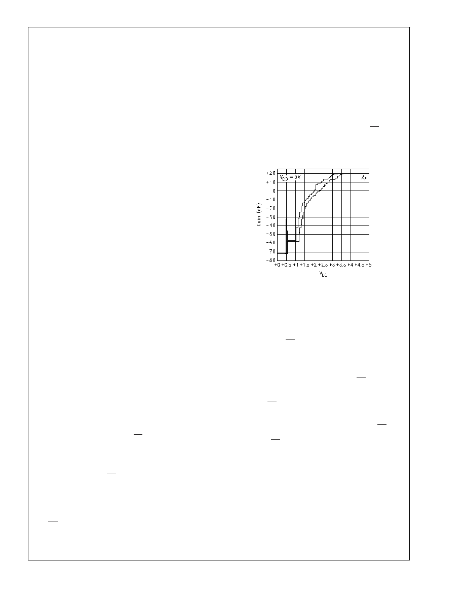
different control voltage to achieve the same gain. Figure 2 is
a curve showing the volume variation of twenty typical
LM4865s as the voltage applied to the DC Vol/SD pin is
varied. For gains greater than unity, the typical part-to-part
variation can be as large as 8dB for the same control volt-
age.
MUTE AND SHUTDOWN FUNCTION
The LM4865’s mute and shutdown functions are controlled
through the DC Vol/SD pin. Mute is activated by applying a
voltage in the range of 500mV to 1V. A typical attenuation of
75dB is achieved is while mute is active. The LM4865’s
micropower shutdown mode turns off the amplifier’s bias
circuitry. The micropower shutdown mode is activated by
applying less than 300mV
DC to the DC Vol/SD pin. When
shutdown is active, they supply current is reduced to 0.7A
(typ). A degree of uncertainty exists when the voltage applied
to the DC Vol/SD pin is in the range of 300mV to 500mV. The
LM4865 can be in mute, still fully powered, or in micropower
shutdown and fully muted. In mute mode, the LM4865 draws
the typical quiescent supply current. The DC Vol/SD pin
should be tied to GND for best shutdown mode performance.
As the DC Vol/SD is increased above 0.5V the amplifier will
follow the attenuation curve in Typical Performance Char-
acteristics.
HP-Sense FUNCTION
Applying a voltage between 4V and V
CC to the LM4865’s
HP-Sense headphone control pin turns off Amp2 and mutes
a bridged-connected load. Quiescent current consumption is
reduced when the IC is in this single-ended mode.
Figure 3 shows the implementation of the LM4865’s head-
phone control function. With no headphones connected to
the headphone jack, the R1-R2 voltage divider sets the
10102547
FIGURE 2. Typical part-to-part gain variation as a
function of DC-Vol control voltage
LM4865
www.national.com
9
相关PDF资料 |
PDF描述 |
|---|---|
| LM4865IBPX | 1 CHANNEL(S), VOLUME CONTROL CIRCUIT, PBGA8 |
| LM4865MDC | 1 CHANNEL(S), VOLUME CONTROL CIRCUIT, UUC |
| LM4865MWC | 1 CHANNEL(S), VOLUME CONTROL CIRCUIT, UUC |
| LM4866MTE/NOPB | 3.2 W, 2 CHANNEL, AUDIO AMPLIFIER, PDSO20 |
| LM4866MT/NOPB | 1.5 W, 2 CHANNEL, AUDIO AMPLIFIER, PDSO20 |
相关代理商/技术参数 |
参数描述 |
|---|---|
| LM4865M | 功能描述:音频放大器 RoHS:否 制造商:STMicroelectronics 产品:General Purpose Audio Amplifiers 输出类型:Digital 输出功率: THD + 噪声: 工作电源电压:3.3 V 电源电流: 最大功率耗散: 最大工作温度: 安装风格:SMD/SMT 封装 / 箱体:TQFP-64 封装:Reel |
| LM4865M | 制造商:Texas Instruments 功能描述:AMP AUDIO/VOLT CONTROL 0.75W 4865 |
| LM4865M/NOPB | 功能描述:音频放大器 RoHS:否 制造商:STMicroelectronics 产品:General Purpose Audio Amplifiers 输出类型:Digital 输出功率: THD + 噪声: 工作电源电压:3.3 V 电源电流: 最大功率耗散: 最大工作温度: 安装风格:SMD/SMT 封装 / 箱体:TQFP-64 封装:Reel |
| LM4865MM | 功能描述:音频放大器 RoHS:否 制造商:STMicroelectronics 产品:General Purpose Audio Amplifiers 输出类型:Digital 输出功率: THD + 噪声: 工作电源电压:3.3 V 电源电流: 最大功率耗散: 最大工作温度: 安装风格:SMD/SMT 封装 / 箱体:TQFP-64 封装:Reel |
| LM4865MM/NOPB | 功能描述:音频放大器 RoHS:否 制造商:STMicroelectronics 产品:General Purpose Audio Amplifiers 输出类型:Digital 输出功率: THD + 噪声: 工作电源电压:3.3 V 电源电流: 最大功率耗散: 最大工作温度: 安装风格:SMD/SMT 封装 / 箱体:TQFP-64 封装:Reel |
发布紧急采购,3分钟左右您将得到回复。