- 您现在的位置:买卖IC网 > PDF目录30754 > LM4865MDC (NATIONAL SEMICONDUCTOR CORP) 1 CHANNEL(S), VOLUME CONTROL CIRCUIT, UUC PDF资料下载
参数资料
| 型号: | LM4865MDC |
| 厂商: | NATIONAL SEMICONDUCTOR CORP |
| 元件分类: | 音频控制 |
| 英文描述: | 1 CHANNEL(S), VOLUME CONTROL CIRCUIT, UUC |
| 封装: | DIE |
| 文件页数: | 17/18页 |
| 文件大小: | 520K |
| 代理商: | LM4865MDC |
Application Information (Continued)
outputs track the voltage applied to the bypass pin. The gain
of the internal amplifiers remains unity until the voltage on
the bypass pin reaches 1/2 V
DD. As soon as the voltage on
the bypass pin is stable, the device becomes fully opera-
tional and the gain is set by the external voltage applied to
the DC Vol/SD pin.
Although the bypass pin current cannot be modified, chang-
ing the size of C
B alters the device’s turn-on time and the
magnitude of
″clicks and pops″. Increasing the value of C
B
reduces the magnitude of turn-on pops. However, this pre-
sents a tradeoff: as the size of C
B increases, the turn-on time
increases. There is a linear relationship between the size of
CB and the turn-on time. Shown below are some typical
turn-on times for various values of C
B:
C
B
T
ON
0.01F
20ms
0.1F
200ms
0.22F
420ms
0.47F
840ms
1.0F
2sec
In order eliminate
″clicks and pops″, all capacitors must be
discharged before turn-on. Rapidly switching V
DD may not
allow the capacitors to fully discharge, which may cause
″clicks and pops″. In a single-ended configuration, the output
coupling capacitor, C
OUT, is of particular concern. This ca-
pacitor discharges through an internal 20k
resistor. De-
pending on the size of C
OUT, the time constant can be
relatively large. To reduce transients in single-ended mode,
an external 1k
-5k resistor can be placed in parallel with
the internal 20k
resistor. The tradeoff for using this resistor
is increased quiescent current.
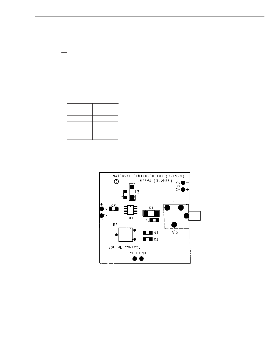
RECOMMENDED PRINTED CIRCUIT BOARD LAYOUT
Figure 4 through Figure 6 show the recommended two-layer
PC board layout that is optimized for the SO-8 packaged
LM4865 and associated external components.
Figure 7
through
Figure 11 show the recommended four-layer PC
board layout for the micro SMD packaged LM4865. A
four-layer board is recommended when using the micro
SMD packaged LM4865: the two inner layers, one con-
nected to the GND pin, the other to the V
DD pin, provide
heatsinking. Both layouts are designed for use with an ex-
ternal 5V supply, 8
speakers, and 32 headphones. The
schematic for both recommended PC board layouts is
Figure
1.
Both circuit boards are easy to use. Apply a 5V supply
voltage and ground to the board’s V
DD and GND pads,
respectively. Connect a speaker with an 8
minimum imped-
ance between the board’s -OUT and +OUT pads. For head-
phone use, the layout has provisions for a headphone jack,
J1. When a jack is connected as shown, inserting a head-
phone plug automatically switches off the external speaker.
DS101025-38
FIGURE 4. Recommended SO PC board layout:
component side silkscreen
LM4865
www.national.com
8
相关PDF资料 |
PDF描述 |
|---|---|
| LM4865MWC | 1 CHANNEL(S), VOLUME CONTROL CIRCUIT, UUC |
| LM4866MTE/NOPB | 3.2 W, 2 CHANNEL, AUDIO AMPLIFIER, PDSO20 |
| LM4866MT/NOPB | 1.5 W, 2 CHANNEL, AUDIO AMPLIFIER, PDSO20 |
| LM4866LQ/NOPB | 3.2 W, 2 CHANNEL, AUDIO AMPLIFIER, PQCC24 |
| LM4866LQX/NOPB | 3.2 W, 2 CHANNEL, AUDIO AMPLIFIER, PQCC24 |
相关代理商/技术参数 |
参数描述 |
|---|---|
| LM4865MM | 功能描述:音频放大器 RoHS:否 制造商:STMicroelectronics 产品:General Purpose Audio Amplifiers 输出类型:Digital 输出功率: THD + 噪声: 工作电源电压:3.3 V 电源电流: 最大功率耗散: 最大工作温度: 安装风格:SMD/SMT 封装 / 箱体:TQFP-64 封装:Reel |
| LM4865MM/NOPB | 功能描述:音频放大器 RoHS:否 制造商:STMicroelectronics 产品:General Purpose Audio Amplifiers 输出类型:Digital 输出功率: THD + 噪声: 工作电源电压:3.3 V 电源电流: 最大功率耗散: 最大工作温度: 安装风格:SMD/SMT 封装 / 箱体:TQFP-64 封装:Reel |
| LM4865MMX | 功能描述:音频放大器 RoHS:否 制造商:STMicroelectronics 产品:General Purpose Audio Amplifiers 输出类型:Digital 输出功率: THD + 噪声: 工作电源电压:3.3 V 电源电流: 最大功率耗散: 最大工作温度: 安装风格:SMD/SMT 封装 / 箱体:TQFP-64 封装:Reel |
| LM4865MMX/NOPB | 功能描述:音频放大器 RoHS:否 制造商:STMicroelectronics 产品:General Purpose Audio Amplifiers 输出类型:Digital 输出功率: THD + 噪声: 工作电源电压:3.3 V 电源电流: 最大功率耗散: 最大工作温度: 安装风格:SMD/SMT 封装 / 箱体:TQFP-64 封装:Reel |
| LM4865MX | 功能描述:音频放大器 RoHS:否 制造商:STMicroelectronics 产品:General Purpose Audio Amplifiers 输出类型:Digital 输出功率: THD + 噪声: 工作电源电压:3.3 V 电源电流: 最大功率耗散: 最大工作温度: 安装风格:SMD/SMT 封装 / 箱体:TQFP-64 封装:Reel |
发布紧急采购,3分钟左右您将得到回复。