- 您现在的位置:买卖IC网 > PDF目录30755 > LM4890ITL/NOPB (NATIONAL SEMICONDUCTOR CORP) 1 W, 1 CHANNEL, AUDIO AMPLIFIER, PBGA9 PDF资料下载
参数资料
| 型号: | LM4890ITL/NOPB |
| 厂商: | NATIONAL SEMICONDUCTOR CORP |
| 元件分类: | 音频/视频放大 |
| 英文描述: | 1 W, 1 CHANNEL, AUDIO AMPLIFIER, PBGA9 |
| 封装: | MICRO, SMD-9 |
| 文件页数: | 26/30页 |
| 文件大小: | 1621K |
| 代理商: | LM4890ITL/NOPB |
第1页第2页第3页第4页第5页第6页第7页第8页第9页第10页第11页第12页第13页第14页第15页第16页第17页第18页第19页第20页第21页第22页第23页第24页第25页当前第26页第27页第28页第29页第30页
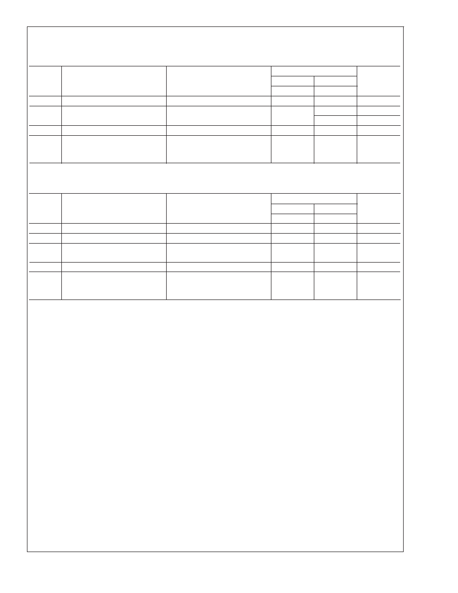
Electrical Characteristics V
The following specifications apply for the circuit shown in Figure 1 unless otherwise specified. Limits apply for T
A =
25C. (Continued)
Symbol
Parameter
Conditions
LM4890
Units
(Limits)
Typical
Limit
(Notes 7, 9)
P
o
Output Power (8
)
THD = 1% (max); f = 1kHz
0.31
0.28
W
T
SD
Thermal Shutdown Temperature
170
150
C(min)
190
C(max)
THD+N
Total Harmonic Distortion + Noise
P
o = 0.15Wrms; f = 1kHz
0.1
%
PSRR
Power Supply Rejection Ratio
V
ripple = 200mV sine p-p
Input terminated with 10 ohms to
ground
56 (f =
217Hz)
62 (f = 1kHz)
45
dB(min)
Electrical Characteristics V
DD = 2.6V
(Notes 1, 2, 8)
The following specifications apply for for the circuit shown in Figure 1 unless otherwise specified. Limits apply for T
A = 25C.
Symbol
Parameter
Conditions
LM4890
Units
(Limits)
Typical
Limit
(Notes 7, 9)
I
DD
Quiescent Power Supply Current
V
IN = 0V, Io = 0A, No Load
2.6
mA (max)
I
SD
Shutdown Current
V
SHUTDOWN = 0V
0.1
A (max)
P
0
Output Power (8
)
Output Power (4
)
THD = 1% (max);f=1kHz
0.2
0.22
W
THD+N
Total Harmonic Distortion + Noise
P
o = 0.1Wrms; f = 1kHz
0.08
%
PSRR
Power Supply Rejection Ratio
V
ripple = 200mV sine p-p
Input Terminated with 10 ohms to
ground
44 (f =
217Hz)
44 (f = 1kHz)
dB
Note 1: All voltages are measured with respect to the ground pin, unless otherwise specified.
Note 2: Absolute Maximum Ratings indicate limits beyond which damage to the device may occur. Operating Ratings indicate conditions for which the device is
functional, but do not guarantee specific performance limits. Electrical Characteristics state DC and AC electrical specifications under particular test conditions which
guarantee specific performance limits. This assumes that the device is within the Operating Ratings. Specifications are not guaranteed for parameters where no limit
is given, however, the typical value is a good indication of device performance.
Note 3: The maximum power dissipation must be derated at elevated temperatures and is dictated by TJMAX, θJA, and the ambient temperature TA. The maximum
allowable power dissipation is PDMAX =(TJMAX–TA)/θJA or the number given in Absolute Maximum Ratings, whichever is lower. For the LM4890, see power derating
curves for additional information.
Note 4: Human body model, 100 pF discharged through a 1.5 k
resistor.
Note 5: Machine Model, 220 pF–240 pF discharged through all pins.
Note 6: Typicals are measured at 25C and represent the parametric norm.
Note 7: Limits are guaranteed to National’s AOQL (Average Outgoing Quality Level).
Note 8: For micro SMD only, shutdown current is measured in a Normal Room Environment. Exposure to direct sunlight will increase ISD by a maximum of 2A.
Note 9: Datasheet min/max specification limits are guaranteed by design, test, or statistical analysis.
Note 10: ROUT is measured from each of the output pins to ground. This value represents the parallel combination of the 10k ohm output resistors and the two 20k
ohm resistors.
Note 11: If the product is in shutdown mode and VDD exceeds 6V (to a max of 8V VDD), then most of the excess current will flow through the ESD protection circuits.
If the source impedance limits the current to a max of 10 ma, then the part will be protected. If the part is enabled when VDD is greater than 5.5V and less than 6.5V,
no damage will occur, although operational life will be reduced. Operation above 6.5V with no current limit will result in permanent damage.
Note 12: All bumps have the same thermal resistance and contribute equally when used to lower thermal resistance. All bumps must be connected to achieve
specified thermal resistance.
Note 13: Maximum power dissipation (PDMAX) in the device occurs at an output power level significantly below full output power. PDMAX can be calculated using
Equation 1 shown in the Application section. It may also be obtained from the power dissipation graphs.
Note 14: PSRR is a function of system gain. Specifications apply to the circuit in Figure 1 where AV = 2. Higher system gains will reduce PSRR value by the amount
of gain increase. A system gain of 10 represents a gain increase of 14dB. PSRR will be reduced by 14dB and applies to all operating voltages.
LM4890
www.national.com
5
相关PDF资料 |
PDF描述 |
|---|---|
| LM4890ITLX/NOPB | 1 W, 1 CHANNEL, AUDIO AMPLIFIER, PBGA9 |
| LM4891MM/NOPB | 1 W, 1 CHANNEL, AUDIO AMPLIFIER, PDSO8 |
| LM4891M/NOPB | 1 W, 1 CHANNEL, AUDIO AMPLIFIER, PDSO8 |
| LM4891LD/NOPB | 1 W, 1 CHANNEL, AUDIO AMPLIFIER, PDSO10 |
| LM4891IBPX/NOPB | 1 W, 1 CHANNEL, AUDIO AMPLIFIER, PBGA8 |
相关代理商/技术参数 |
参数描述 |
|---|---|
| LM4890ITLX | 制造商:NSC 制造商全称:National Semiconductor 功能描述:1 Watt Audio Power Amplifier |
| LM4890ITLX/NOPB | 功能描述:音频放大器 RoHS:否 制造商:STMicroelectronics 产品:General Purpose Audio Amplifiers 输出类型:Digital 输出功率: THD + 噪声: 工作电源电压:3.3 V 电源电流: 最大功率耗散: 最大工作温度: 安装风格:SMD/SMT 封装 / 箱体:TQFP-64 封装:Reel |
| LM4890ITP | 制造商:Texas Instruments 功能描述:AMP AUDIO CELLULAR 1W SMD 4890 |
| LM4890ITP/NOPB | 功能描述:IC AMP AUDIO PWR 1W MONO 8USMD RoHS:是 类别:集成电路 (IC) >> 线性 - 音頻放大器 系列:Boomer® 产品培训模块:Lead (SnPb) Finish for COTS Obsolescence Mitigation Program 标准包装:2,500 系列:DirectDrive® 类型:H 类 输出类型:耳机,2-通道(立体声) 在某负载时最大输出功率 x 通道数量:35mW x 2 @ 16 欧姆 电源电压:1.62 V ~ 1.98 V 特点:I²C,麦克风,静音,短路保护,音量控制 安装类型:表面贴装 供应商设备封装:25-WLP(2.09x2.09) 封装/外壳:25-WFBGA,WLCSP 包装:带卷 (TR) |
| LM4890ITPX/NOPB | 功能描述:音频放大器 RoHS:否 制造商:STMicroelectronics 产品:General Purpose Audio Amplifiers 输出类型:Digital 输出功率: THD + 噪声: 工作电源电压:3.3 V 电源电流: 最大功率耗散: 最大工作温度: 安装风格:SMD/SMT 封装 / 箱体:TQFP-64 封装:Reel |
发布紧急采购,3分钟左右您将得到回复。