- 您现在的位置:买卖IC网 > PDF目录32307 > LM4891MX/NOPB (NATIONAL SEMICONDUCTOR CORP) 1 W, 1 CHANNEL, AUDIO AMPLIFIER, PDSO8 PDF资料下载
参数资料
| 型号: | LM4891MX/NOPB |
| 厂商: | NATIONAL SEMICONDUCTOR CORP |
| 元件分类: | 音频/视频放大 |
| 英文描述: | 1 W, 1 CHANNEL, AUDIO AMPLIFIER, PDSO8 |
| 封装: | SOIC-8 |
| 文件页数: | 2/23页 |
| 文件大小: | 674K |
| 代理商: | LM4891MX/NOPB |
Typical Performance Characteristics (Continued)
Application Information
BRIDGE CONFIGURATION EXPLANATION
As shown in
Figure 1, the LM4891 has two operational
amplifiers internally, allowing for a few different amplifier
configurations. The first amplifier’s gain is externally config-
urable, while the second amplifier is internally fixed in a
unity-gain, inverting configuration. The closed-loop gain of
the first amplifier is set by selecting the ratio of R
f to Ri while
the second amplifier’s gain is fixed by the two internal 20 k
resistors.
Figure 1 shows that the output of amplifier one
serves as the input to amplifier two which results in both
amplifiers producing signals identical in magnitude, but out
of phase by 180. Consequently, the differential gain for the
IC is
A
VD= 2 *(Rf/Ri)
By driving the load differentially through outputs Vo1 and
Vo2, an amplifier configuration commonly referred to as
“bridged mode” is established. Bridged mode operation is
different from the classical single-ended amplifier configura-
tion where one side of the load is connected to ground.
A bridge amplifier design has a few distinct advantages over
the single-ended configuration, as it provides differential
drive to the load, thus doubling output swing for a specified
supply voltage. Four times the output power is possible as
compared to a single-ended amplifier under the same con-
ditions. This increase in attainable output power assumes
that the amplifier is not current limited or clipped. In order to
choose an amplifier’s closed-loop gain without causing ex-
cessive clipping, please refer to the Audio Power Amplifier
Design section.
A bridge configuration, such as the one used in LM4891,
also creates a second advantage over single-ended amplifi-
ers. Since the differential outputs, Vo1 and Vo2, are biased
at half-supply, no net DC voltage exists across the load. This
eliminates the need for an output coupling capacitor which is
required in a single supply, single-ended amplifier configura-
tion. Without an output coupling capacitor, the half-supply
bias across the load would result in both increased internal
IC power dissipation and also possible loudspeaker damage.
EXPOSED-DAP PACKAGE PCB MOUNTING
CONSIDERATIONS FOR THE LM4891LD
The LM4891LD’s exposed-DAP (die attach paddle) package
(LD) provides a low thermal resistance between the die and
the PCB to which the part is mounted and soldered. The
LM4891LD package should have its DAP soldered to the
grounded copper pad (heatsink) under the LM4891LD (the
NC pins, no connect, and ground pins should also be directly
connected to this copper pad-heatsink area). The area of the
copper pad (heatsink) can be determined from the LD Power
Derating graph. If the multiple layer copper heatsink areas
are used, then these inner layer or backside copper heatsink
areas should be connected to each other with 4 (2 x 2) vias.
The diameter for these vias should be between 0.013 inches
and 0.02 inches with a 0.050inch pitch-spacing. Ensure
efficient thermal conductivity by plating through and solder-
filling the vias. Further detailed information concerning PCB
layout, fabrication, and mounting an LLP package is avail-
able from National Semiconductor’s Package Engineering
Group under application note AN1187.
POWER DISSIPATION
Power dissipation is a major concern when designing a
successful amplifier, whether the amplifier is bridged or
single-ended. A direct consequence of the increased power
delivered to the load by a bridge amplifier is an increase in
internal power dissipation. Since the LM4891 has two opera-
tional amplifiers in one package, the maximum internal
power dissipation is 4 times that of a single-ended amplifier.
The maximum power dissipation for a given application can
be derived from the power dissipation graphs or from Equa-
tion 1.
P
DMAX = 4*(VDD)
2/(2
π2R
L)
(1)
It is critical that the maximum junction temperature (T
JMAX)
of 150C is not exceeded. T
JMAX can be determined from the
power derating curves by using P
DMAX and the PC board foil
area. By adding additional copper foil, the thermal resistance
of the application can be reduced from a free air value of
150C/W, resulting in higher P
DMAX. Additional copper foil
can be added to any of the leads connected to the LM4891.
It is especially effective when connected to V
DD, GND, and
the output pins. Refer to the application information on the
LM4891 reference design board for an example of good heat
sinking. If T
JMAX
still exceeds 150C, then additional
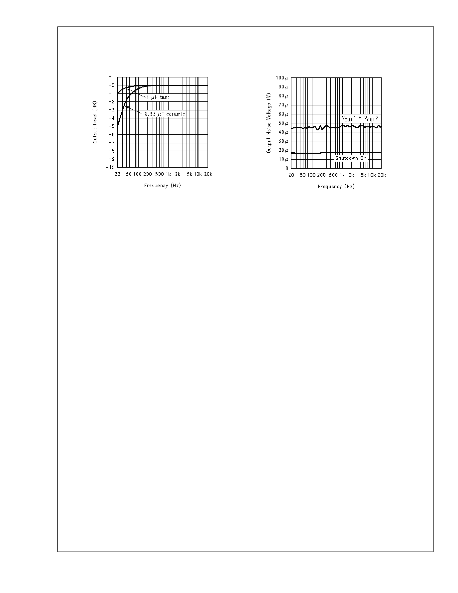
Frequency Response vs
Input Capacitor Size
DS200074-54
Noise Floor
DS200074-56
LM4891
www.national.com
10
相关PDF资料 |
PDF描述 |
|---|---|
| LM4891LDX/NOPB | 1 W, 1 CHANNEL, AUDIO AMPLIFIER, PDSO10 |
| LM4898MMXNPAU | 1 W, 1 CHANNEL, AUDIO AMPLIFIER, PDSO10 |
| LM4898ITLX/NOPB | 1 W, 1 CHANNEL, AUDIO AMPLIFIER, PBGA9 |
| LM4904ITL/NOPB | 1.07 W, 1 CHANNEL, AUDIO AMPLIFIER, PBGA8 |
| LM4904ITLX/NOPB | 1.07 W, 1 CHANNEL, AUDIO AMPLIFIER, PBGA8 |
相关代理商/技术参数 |
参数描述 |
|---|---|
| LM4892 | 制造商:NSC 制造商全称:National Semiconductor 功能描述:1 Watt Audio Power Amplifier with Headphone Sense |
| LM48920B WAF | 制造商:Texas Instruments 功能描述: |
| LM4892B E WAF | 制造商:Texas Instruments 功能描述: |
| LM4892BUPN E WAF | 制造商:Texas Instruments 功能描述: |
| LM4892IBP | 功能描述:IC AMP AUDIO PWR 1W MONO 8USMD RoHS:否 类别:集成电路 (IC) >> 线性 - 音頻放大器 系列:Boomer® 产品培训模块:Lead (SnPb) Finish for COTS Obsolescence Mitigation Program 标准包装:2,500 系列:DirectDrive® 类型:H 类 输出类型:耳机,2-通道(立体声) 在某负载时最大输出功率 x 通道数量:35mW x 2 @ 16 欧姆 电源电压:1.62 V ~ 1.98 V 特点:I²C,麦克风,静音,短路保护,音量控制 安装类型:表面贴装 供应商设备封装:25-WLP(2.09x2.09) 封装/外壳:25-WFBGA,WLCSP 包装:带卷 (TR) |
发布紧急采购,3分钟左右您将得到回复。