- 您现在的位置:买卖IC网 > PDF目录30757 > LM6162MW8 (NATIONAL SEMICONDUCTOR CORP) 1 CHANNEL, VIDEO AMPLIFIER, UUC PDF资料下载
参数资料
| 型号: | LM6162MW8 |
| 厂商: | NATIONAL SEMICONDUCTOR CORP |
| 元件分类: | 音频/视频放大 |
| 英文描述: | 1 CHANNEL, VIDEO AMPLIFIER, UUC |
| 封装: | WAFER |
| 文件页数: | 9/14页 |
| 文件大小: | 442K |
| 代理商: | LM6162MW8 |
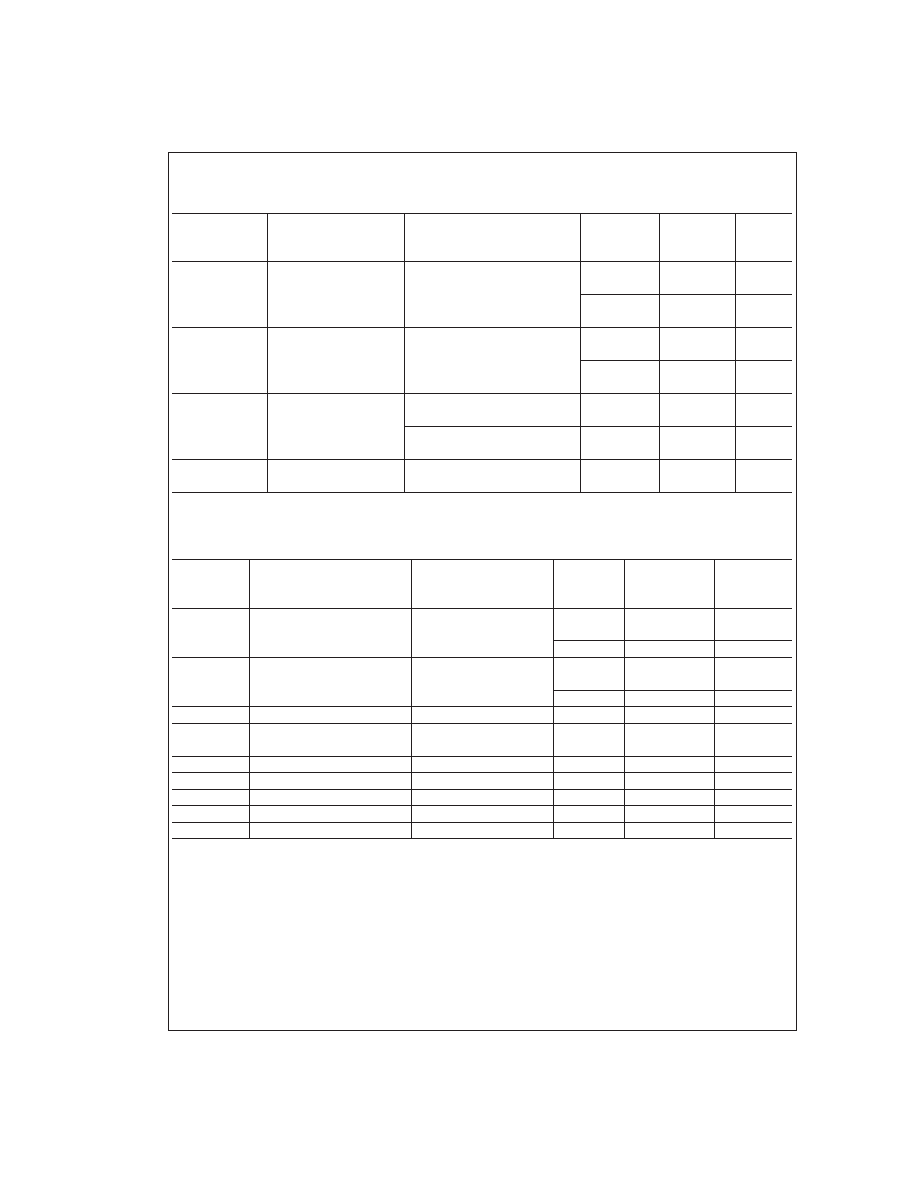
DC Electrical Characteristics (Continued)
These limits apply for supply voltage = ±15V, V
CM = 0V, and RL ≥ 100 k, unless otherwise specified. Limits in standard
typeface are for T
A = TJ = 25C; limits in boldface type apply over the Operating Temperature Range.
Typical
(Note 7)
LM6162
Symbol
Parameter
Conditions
Limit
Units
(Note 8)
V
O
Output Voltage
Supply = ±15V, R
L = 2k
+14.2
+13.5
V
Swing
+13.3
min
13.4
13.0
V
12.7
max
V
O
Output Voltage Swing
Supply = +5V and
4.2
3.5
V
R
L = 2k (Note 10)
3.3
min
1.3
1.7
V
2.0
max
I
OSC
Output Short
Sourcing
65
30
mA
Circuit Current
20
min
Sinking
65
30
mA
20
min
I
S
Supply Current
5.0
6.5
mA
6.8
max
AC Electrical Characteristics
These limits apply for supply voltage = ±15V, V
CM = 0V, RL ≥ 100 k, and CL ≤ 5 pF, unless otherwise specified. Limits
in standard typeface are for T
A = TJ = 25C; limits in boldface type apply over the Operating Temperature Range.
Typical
(Note
7)
LM6162
Symbol
Parameter
Conditions
Limit
Units
(Note 8)
GBW
Gain-Bandwidth Product
f = 20 MHz
100
80
MHz
55
min
Supply = ±5V
70
MHz
SR
Slew Rate
A
V = +2 (Note 11)
300
200
V/s
180
min
Supply = ±5V
200
V/s
PBW
Power Bandwidth
V
OUT = 20 VPP
4.5
MHz
t
s
Settling Time
10V step, to 0.1%
100
ns
A
V = 1, RL = 2k
φ
m
Phase Margin
A
V = +2
45
deg
Differential Gain
NTSC, A
V = +2
<0.1
%
Differential Phase
NTSC, A
V = +2
<0.1
deg
e
n
Input Noise Voltage
f = 10 kHz
10
nV/
√Hz
i
n
Input Noise Current
f = 10 kHz
1.2
pA/
√Hz
Note 1: Absolute maximum ratings indicate limits beyond which damage to the component may occur. Electrical specifications do not apply when operating the de-
vice beyond its rated operating conditions.
Note 2: The ESD protection circuitry between the inputs will begin to conduct when the differential input voltage reaches 8V.
Note 3: a) In addition, the voltage between the V+ pin and either input pin must not exceed 36V.
b) When the voltage applied to an input pin is driven more than 3V below the negative supply pin voltage, a substrate diode begins to conduct. Current through this
pin must then be kept less than 20 mA to limit damage from self-heating.
Note 4: Although the output current is internally limited, continuous short-circuit operation at elevated ambient temperature can result in exceeding the maximum al-
lowed junction temperature of 150C.
Note 5: This value is the average voltage that the weakest pin combinations can withstand and still conform to the datasheet limits. The test circuit used consists
of the human body model, 100 pF in series with 1500
.
Note 6: The typical thermal resistance, junction-to-ambient, of the molded plastic DIP (N package) is 105C/W. For the molded plastic SO (M package), use
155C/W. All numbers apply for packages soldered directly into a printed circuit board.
Note 7: Typical values are for TJ = 25C, and represent the most likely parametric norm.
Note 8: Limits are guaranteed, by testing or correlation.
www.national.com
4
相关PDF资料 |
PDF描述 |
|---|---|
| LM6162W/883X | 1 CHANNEL, VIDEO AMPLIFIER, CDFP10 |
| 5962-9216501MPX | 1 CHANNEL, VIDEO AMPLIFIER, CDIP8 |
| LM6162WG-QMLV | VIDEO AMPLIFIER, CDSO10 |
| 9216501MPA | OP-AMP, 8000 uV OFFSET-MAX, 100 MHz BAND WIDTH, CDIP8 |
| 9216501MXA | OP-AMP, 8000 uV OFFSET-MAX, 100 MHz BAND WIDTH, CDSO10 |
相关代理商/技术参数 |
参数描述 |
|---|---|
| LM6162N | 制造商:Texas Instruments 功能描述:OP AMP HIGH-SPEED |
| LM6162W/883 | 制造商:NSC 制造商全称:National Semiconductor 功能描述:High Speed Operational Amplifier |
| LM6162WG/883 | 制造商:NSC 制造商全称:National Semiconductor 功能描述:High Speed Operational Amplifier |
| LM6164 | 制造商:NSC 制造商全称:National Semiconductor 功能描述:High Speed Operational Amplifier |
| LM6164E/883 | 制造商:Rochester Electronics LLC 功能描述:- Bulk 制造商:Texas Instruments 功能描述: |
发布紧急采购,3分钟左右您将得到回复。