- 您现在的位置:买卖IC网 > PDF目录30757 > LM6172AMJ-MLS (NATIONAL SEMICONDUCTOR CORP) VIDEO AMPLIFIER, CDIP8 PDF资料下载
参数资料
| 型号: | LM6172AMJ-MLS |
| 厂商: | NATIONAL SEMICONDUCTOR CORP |
| 元件分类: | 音频/视频放大 |
| 英文描述: | VIDEO AMPLIFIER, CDIP8 |
| 封装: | CERDIP-8 |
| 文件页数: | 5/20页 |
| 文件大小: | 560K |
| 代理商: | LM6172AMJ-MLS |
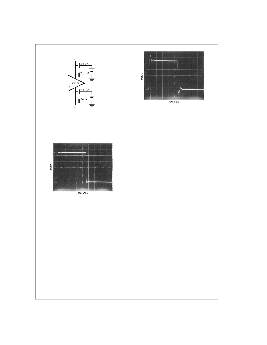
Power Supply Bypassing (Continued)
Termination
In high frequency applications, reflections occur if signals
are not properly terminated.
Figure 6 shows a properly termi-
nated signal while
Figure 7 shows an improperly terminated
signal.
To minimize reflection, coaxial cable with matching charac-
teristic impedance to the signal source should be used. The
other end of the cable should be terminated with the same
value terminator or resistor. For the commonly used cables,
RG59 has 75
characteristic impedance, and RG58 has
50
characteristic impedance.
Power Dissipation
The maximum power allowed to dissipate in a device is de-
fined as:
P
D = (TJ(max) TA)/θJA
Where P
D is the power dissipation in a device
T
J(max) is the maximum junction temperature
T
A is the ambient temperature
θ
JA is the thermal resistance of a particular package
For example, for the LM6172 in a SO-8 package, the maxi-
mum power dissipation at 25C ambient temperature is
780 mW.
Thermal resistance,
θ
JA, depends on parameters such as
die size, package size and package material. The smaller
the die size and package, the higher
θ
JA becomes. The 8-pin
DIP package has a lower thermal resistance (95C/W) than
that of 8-pin SO (160C/W). Therefore, for higher dissipation
capability, use an 8-pin DIP package.
The total power dissipated in a device can be calculated as:
P
D = PQ +PL
P
Q is the quiescent power dissipated in a device with no load
connected at the output. P
L is the power dissipated in the de-
vice with a load connected at the output; it is not the power
dissipated by the load.
Furthermore,
P
Q:
=
supply current x total supply voltage with no load
P
L:
=
output current x (voltage difference between sup-
ply voltage and output voltage of the same supply)
For example, the total power dissipated by the LM6172 with
V
S = ±15V and both channels swinging output voltage of
10V into 1 k
is
P
D:
=
P
Q +PL
:
=
2[(2.3 mA)(30V)] + 2[(10 mA)(15V 10V)]
:
=
138 mW + 100 mW
:
=
238 mW
DS012581-47
FIGURE 5. Power Supply Bypassing
DS012581-53
FIGURE 6. Properly Terminated Signal
DS012581-54
FIGURE 7. Improperly Terminated Signal
www.national.com
13
相关PDF资料 |
PDF描述 |
|---|---|
| LM6172AMWGRQML | VIDEO AMPLIFIER, CDSO16 |
| LM6172AMJRQML | VIDEO AMPLIFIER, CDIP8 |
| LM6172MDC | 2 CHANNEL, VIDEO AMPLIFIER, UUC |
| LM6181AIM-8X | VIDEO AMPLIFIER, PDSO8 |
| LM6181AIMX | VIDEO AMPLIFIER, PDSO16 |
相关代理商/技术参数 |
参数描述 |
|---|---|
| LM6172AMJ-QML | 制造商:NSC 制造商全称:National Semiconductor 功能描述:Dual High Speed, Low Power, Low Distortion, Voltage Feedback Amplifiers |
| LM6172AMWGFQMLV | 制造商:TI 制造商全称:Texas Instruments 功能描述:Dual High Speed, Low Power, Low Distortion, Voltage Feedback Amplifiers |
| LM6172AMWG-QML | 制造商:National Semiconductor Corporation 功能描述:OP Amp Dual Volt Fdbk ±18V/36V 16-Pin CPAK 制造商:National Semiconductor 功能描述:OP Amp Dual Volt Fdbk ±18V/36V 16-Pin CPAK |
| LM6172IM | 功能描述:运算放大器 - 运放 RoHS:否 制造商:STMicroelectronics 通道数量:4 共模抑制比(最小值):63 dB 输入补偿电压:1 mV 输入偏流(最大值):10 pA 工作电源电压:2.7 V to 5.5 V 安装风格:SMD/SMT 封装 / 箱体:QFN-16 转换速度:0.89 V/us 关闭:No 输出电流:55 mA 最大工作温度:+ 125 C 封装:Reel |
| LM6172IM/NOPB | 功能描述:运算放大器 - 运放 Dual High Speed,Low Pwr Amp RoHS:否 制造商:STMicroelectronics 通道数量:4 共模抑制比(最小值):63 dB 输入补偿电压:1 mV 输入偏流(最大值):10 pA 工作电源电压:2.7 V to 5.5 V 安装风格:SMD/SMT 封装 / 箱体:QFN-16 转换速度:0.89 V/us 关闭:No 输出电流:55 mA 最大工作温度:+ 125 C 封装:Reel |
发布紧急采购,3分钟左右您将得到回复。