- 您现在的位置:买卖IC网 > PDF目录2153 > LMC6484AIN/NOPB (National Semiconductor)IC OP AMP QUAD CMOS R-R 14-DIP PDF资料下载
参数资料
| 型号: | LMC6484AIN/NOPB |
| 厂商: | National Semiconductor |
| 文件页数: | 5/24页 |
| 文件大小: | 0K |
| 描述: | IC OP AMP QUAD CMOS R-R 14-DIP |
| 标准包装: | 25 |
| 放大器类型: | 通用 |
| 电路数: | 4 |
| 输出类型: | 满摆幅 |
| 转换速率: | 1.3 V/µs |
| 增益带宽积: | 1.5MHz |
| 电流 - 输入偏压: | 0.02pA |
| 电压 - 输入偏移: | 110µV |
| 电流 - 电源: | 2.6mA |
| 电流 - 输出 / 通道: | 30mA |
| 电压 - 电源,单路/双路(±): | 3 V ~ 15.5 V,±1.5 V ~ 7.75 V |
| 工作温度: | -40°C ~ 85°C |
| 安装类型: | 通孔 |
| 封装/外壳: | 14-DIP(0.300",7.62mm) |
| 供应商设备封装: | 14-DIP |
| 包装: | 管件 |
| 产品目录页面: | 1266 (CN2011-ZH PDF) |
| 其它名称: | *LMC6484AIN *LMC6484AIN/NOPB LMC6484AIN |
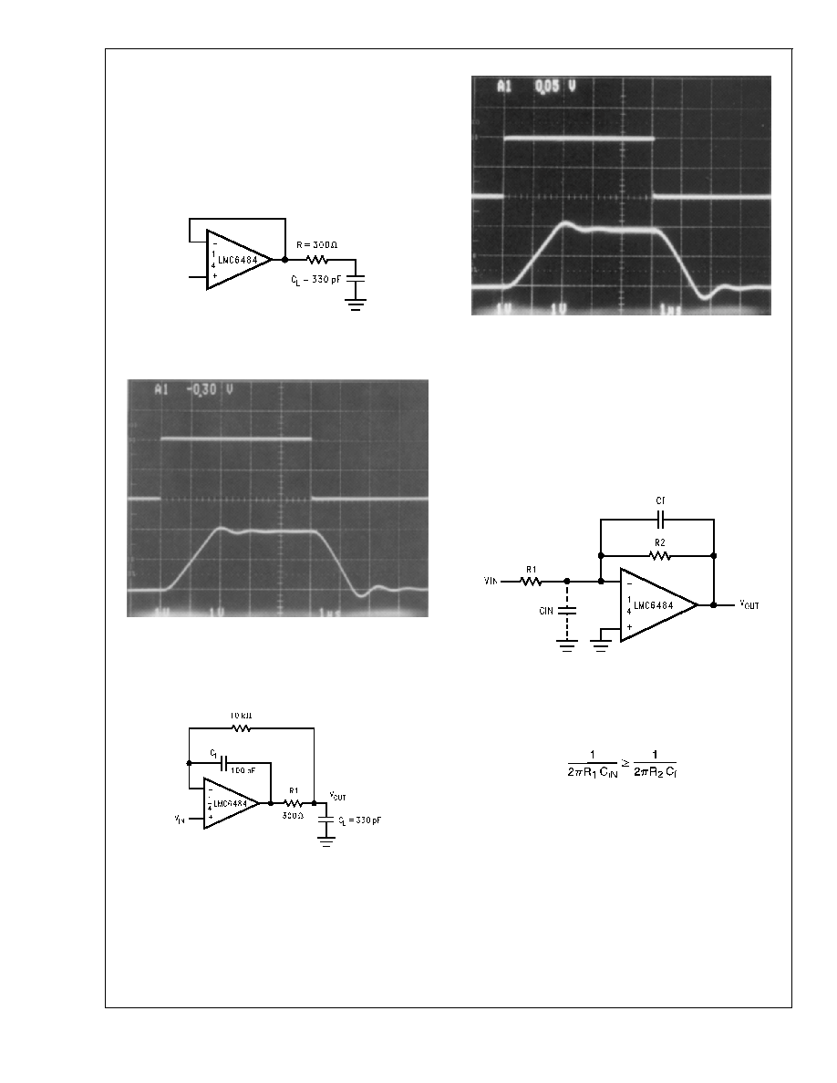
Application Information (Continued)
loading reduces the phase margin of op-amps. The combi-
nation of the op-amp’s output impedance and the capacitive
load induces phase lag. This results in either an under-
damped pulse response or oscillation.
Capacitive load compensation can be accomplished using
resistive isolation as shown in
Figure 4. This simple tech-
nique is useful for isolating the capacitive input of multiplex-
ers and A/D converters.
Improved frequency response is achieved by indirectly driv-
ing capacitive loads as shown in
Figure 6.
R1 and C1 serve to counteract the loss of phase margin by
feeding forward the high frequency component of the output
signal back to the amplifier’s inverting input, thereby preserv-
ing phase margin in the overall feedback loop. The values of
R1 and C1 are experimentally determined for the desired
pulse response. The resulting pulse response can be seen in
Figure 7.
5.0 Compensating for Input Capacitance
It is quite common to use large values of feedback resis-
tance with amplifiers that have ultra-low input current, like
the LMC6484. Large feedback resistors can react with small
values of input capacitance due to transducers, photo-
diodes, and circuit board parasitics to reduce phase
margins.
The effect of input capacitance can be compensated for by
adding a feedback capacitor. The feedback capacitor (as in
Figure 8 ), C
f, is first estimated by:
or
R
1 CIN ≤ R2 Cf
which typically provides significant overcompensation.
Printed circuit board stray capacitance may be larger or
smaller than that of a breadboard, so the actual optimum
value for C
f may be different. The values of Cf should be
checked on the actual circuit. (Refer to the LMC660 quad
CMOS amplifier data sheet for a more detailed discussion.)
6.0 Printed-Circuit-Board Layout for High-Impedance
Work
It is generally recognized that any circuit which must operate
with less than 1000 pA of leakage current requires special
layout of the PC board. when one wishes to take advantage
DS011714-17
FIGURE 4. Resistive Isolation
of a 330 pF Capacitive Load
DS011714-18
FIGURE 5. Pulse Response of
the LMC6484 Circuit in
Figure 4
DS011714-15
FIGURE 6. LMC6484 Non-Inverting Amplifier,
Compensated to Handle a 330 pF Capacitive Load
DS011714-16
FIGURE 7. Pulse Response of
LMC6484 Circuit in
Figure 6
DS011714-19
FIGURE 8. Canceling the Effect of Input Capacitance
LMC6484
www.national.com
12
相关PDF资料 |
PDF描述 |
|---|---|
| LMC7101BYM5 TR | IC OPAMP STD 500KHZ SOT23-5 |
| LMH6619MAX/NOPB | IC AMP DUAL RRIO 130MHZ 8-SOIC |
| LMH6644MTX/NOPB | IC OP AMP R-R LP 3V 75MA 14TSSOP |
| LMP8270MAX/NOPB | IC AMP PREC VOLT DIFF 8-SOIC |
| LMP8277MAX/NOPB | IC AMP PREC VOLT DIFF 8-SOIC |
相关代理商/技术参数 |
参数描述 |
|---|---|
| LMC6484AMJ | 制造商:TI 制造商全称:Texas Instruments 功能描述:LMC6484 CMOS Quad Rail-to-Rail Input and Output Operational Amplifier |
| LMC6484AMJ/883 | 制造商:Texas Instruments 功能描述:5962-9453402MCA CMOS QUAD RAIL TO RAIL I - Rail/Tube |
| LMC6484AMWG/883 | 制造商:Texas Instruments 功能描述: |
| LMC6484IM | 功能描述:运算放大器 - 运放 RoHS:否 制造商:STMicroelectronics 通道数量:4 共模抑制比(最小值):63 dB 输入补偿电压:1 mV 输入偏流(最大值):10 pA 工作电源电压:2.7 V to 5.5 V 安装风格:SMD/SMT 封装 / 箱体:QFN-16 转换速度:0.89 V/us 关闭:No 输出电流:55 mA 最大工作温度:+ 125 C 封装:Reel |
| LMC6484IM | 制造商:Texas Instruments 功能描述:IC OP AMP QUAD CMOS 6484 SOIC14 |
发布紧急采购,3分钟左右您将得到回复。