- 您现在的位置:买卖IC网 > PDF目录3587 > LMC6484IMX/NOPB (National Semiconductor)IC OP AMP QUAD CMOS R-R 14-SOIC PDF资料下载
参数资料
| 型号: | LMC6484IMX/NOPB |
| 厂商: | National Semiconductor |
| 文件页数: | 21/24页 |
| 文件大小: | 0K |
| 描述: | IC OP AMP QUAD CMOS R-R 14-SOIC |
| 标准包装: | 2,500 |
| 放大器类型: | 通用 |
| 电路数: | 4 |
| 输出类型: | 满摆幅 |
| 转换速率: | 1.3 V/µs |
| 增益带宽积: | 1.5MHz |
| 电流 - 输入偏压: | 0.02pA |
| 电压 - 输入偏移: | 110µV |
| 电流 - 电源: | 2.6mA |
| 电流 - 输出 / 通道: | 30mA |
| 电压 - 电源,单路/双路(±): | 3 V ~ 15.5 V,±1.5 V ~ 7.75 V |
| 工作温度: | -40°C ~ 85°C |
| 安装类型: | 表面贴装 |
| 封装/外壳: | 14-SOIC(0.154",3.90mm 宽) |
| 供应商设备封装: | 14-SOICN |
| 包装: | 带卷 (TR) |
| 产品目录页面: | 1266 (CN2011-ZH PDF) |
| 其它名称: | *LMC6484IMX LMC6484IMX LMC6484IMXTR |
AC Electrical Characteristics (Continued)
Note 2: Human body model, 1.5 k
in series with 100 pF. All pins rated per method 3015.6 of MIL-STD-883. This is a class 2 device rating.
Note 3: Applies to both single supply and split-supply operation. Continuous short circuit operation at elevated ambient temperature can result in exceeding the
maximum allowed junction temperature of 150C. Output currents in excess of ±30 mA over long term may adversely affect reliability.
Note 4: The maximum power dissipation is a function of TJ(max), θJA, and TA. The maximum allowable power dissipation at any ambient temperature is
PD =(TJ(max) TA)/θJA. All numbers apply for packages soldered directly into a PC board.
Note 5: Typical Values represent the most likely parametric norm.
Note 6: All limits are guaranteed by testing or statistical analysis.
Note 7: V+ = 15V, VCM = 7.5V and RL connected to 7.5V. For Sourcing tests, 7.5V ≤ VO ≤ 11.5V. For Sinking tests, 3.5V ≤ VO ≤ 7.5V.
Note 8: Do not short circuit output to V+, when V+ is greater than 13V or reliability will be adversely affected.
Note 9: V+ = 15V. Connected as Voltage Follower with 10V step input. Number specified is the slower of either the positive or negative slew rates.
Note 10: Input referred, V+ = 15V and RL = 100 k connected to 7.5V. Each amp excited in turn with 1 kHz to produce VO =12 VPP.
Note 11: Connected as Voltage Follower with 2V step input. Number specified is the slower of either the positive or negative slew rates.
Note 12: Limiting input pin current is only necessary for input voltages that exceed absolute maximum input voltage ratings.
Note 13: Guaranteed limits are dictated by tester limitations and not device performance. Actual performance is reflected in the typical value.
Note 14: For guaranteed Military Temperature Range parameters see RETSMC6484X.
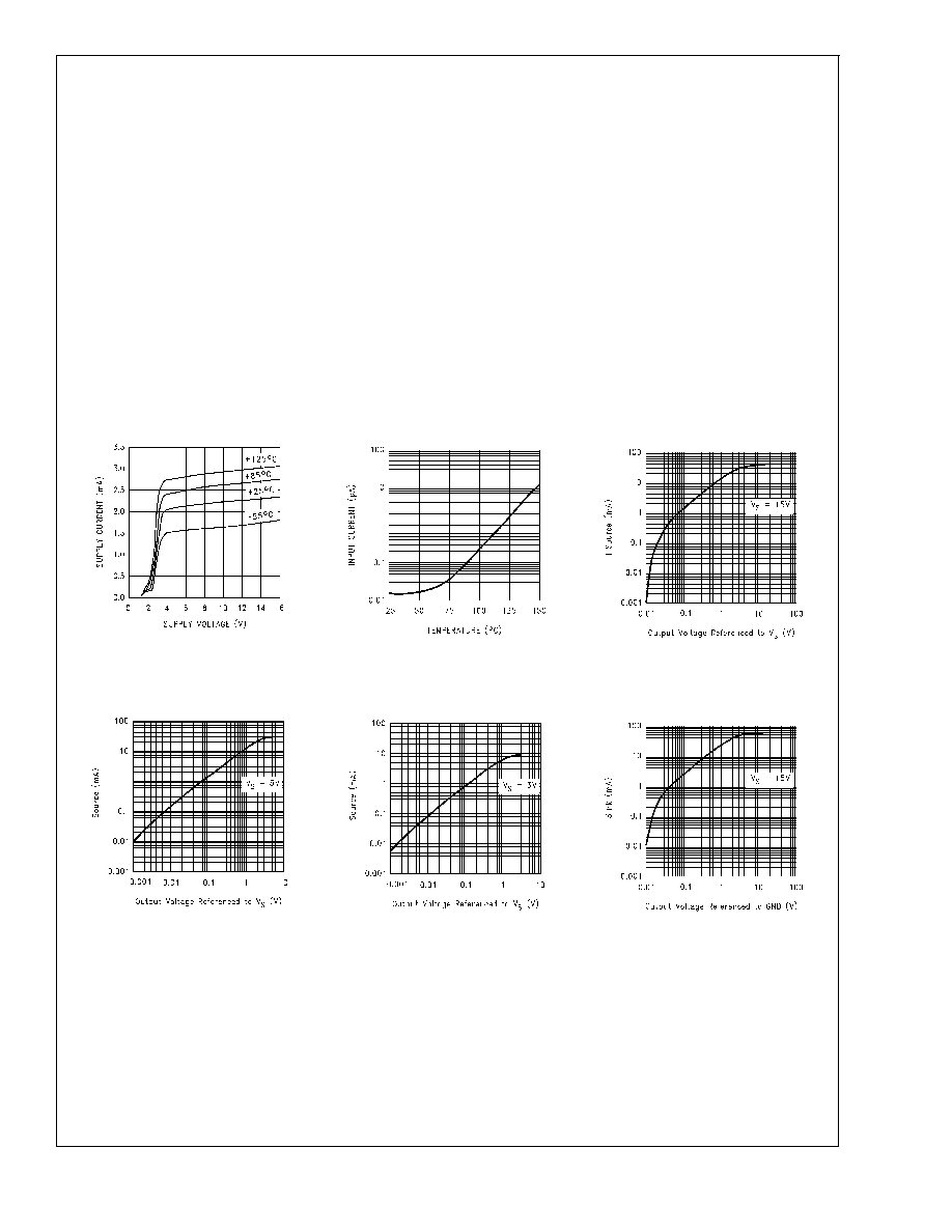
Typical Performance Characteristics V
S = +15V, Single Supply, TA = 25C unless otherwise
specified
Supply Current vs
Supply Voltage
DS011714-39
Input Current vs
Temperature
DS011714-40
Sourcing Current vs
Output Voltage
DS011714-41
Sourcing Current vs
Output Voltage
DS011714-42
Sourcing Current vs
Output Voltage
DS011714-43
Sinking Current vs
Output Voltage
DS011714-44
LMC6484
www.national.com
5
相关PDF资料 |
PDF描述 |
|---|---|
| TSW-130-23-T-D | CONN HEADER 60POS .100" DUAL TIN |
| TSW-141-23-L-S | CONN HEADER 41POS .100" SGL GOLD |
| 5-794680-2 | 22P MICRO MNL ASSY VRT THRU LF |
| TSW-126-08-T-D-RA | CONN HEADER 52PS .100 DL R/A TIN |
| ISL28276FBZ-T7 | IC OPAMP DUAL RRIO PREC 8-SOIC |
相关代理商/技术参数 |
参数描述 |
|---|---|
| LMC6484IN | 功能描述:运算放大器 - 运放 RoHS:否 制造商:STMicroelectronics 通道数量:4 共模抑制比(最小值):63 dB 输入补偿电压:1 mV 输入偏流(最大值):10 pA 工作电源电压:2.7 V to 5.5 V 安装风格:SMD/SMT 封装 / 箱体:QFN-16 转换速度:0.89 V/us 关闭:No 输出电流:55 mA 最大工作温度:+ 125 C 封装:Reel |
| LMC6484IN | 制造商:Texas Instruments 功能描述:IC OP AMP QUAD CMOS 6484 DIP14 |
| LMC6484IN/NOPB | 功能描述:运算放大器 - 运放 CMOS Quad R/R I/O Op Amp RoHS:否 制造商:STMicroelectronics 通道数量:4 共模抑制比(最小值):63 dB 输入补偿电压:1 mV 输入偏流(最大值):10 pA 工作电源电压:2.7 V to 5.5 V 安装风格:SMD/SMT 封装 / 箱体:QFN-16 转换速度:0.89 V/us 关闭:No 输出电流:55 mA 最大工作温度:+ 125 C 封装:Reel |
| LMC6484MN | 制造商:NSC 制造商全称:National Semiconductor 功能描述:CMOS Quad Rail-to-Rail Input and Output Operational Amplifier |
| LMC6484N | 制造商:未知厂家 制造商全称:未知厂家 功能描述:CMOS Quad Rail-to-Rail Input and Output Operational Amplifier(970.84 k) |
发布紧急采购,3分钟左右您将得到回复。