- 您现在的位置:买卖IC网 > PDF目录30759 > LMH6702J-QML/NOPB (NATIONAL SEMICONDUCTOR CORP) 1 CHANNEL, VIDEO AMPLIFIER, CDIP8 PDF资料下载
参数资料
| 型号: | LMH6702J-QML/NOPB |
| 厂商: | NATIONAL SEMICONDUCTOR CORP |
| 元件分类: | 音频/视频放大 |
| 英文描述: | 1 CHANNEL, VIDEO AMPLIFIER, CDIP8 |
| 封装: | CERAMIC, DIP-8 |
| 文件页数: | 13/13页 |
| 文件大小: | 780K |
| 代理商: | LMH6702J-QML/NOPB |
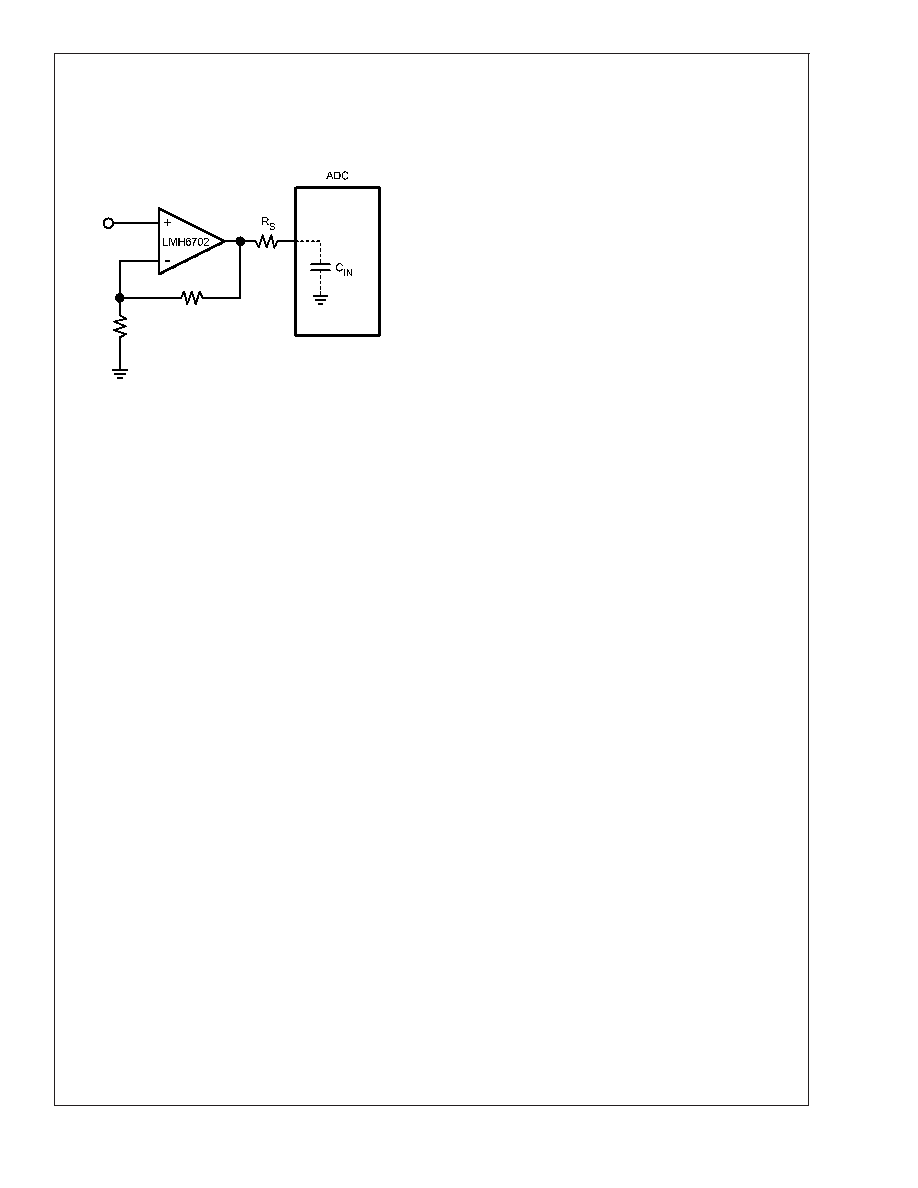
Application Section (Continued)
CAPACITIVE LOAD DRIVE
Figure 4 shows a typical application using the LMH6702 to
drive an ADC.
The series resistor, R
S, between the amplifier output and the
ADC input is critical to achieving best system performance.
This load capacitance, if applied directly to the output pin,
can quickly lead to unacceptable levels of ringing in the
pulse response. The plot of "R
S and Settling Time vs. CL"in
the Typical Performance Characteristics section is an excel-
lent starting point for selecting R
S. The value derived in that
plot minimizes the step settling time into a fixed discrete
capacitive load with the output driving a very light resistive
load (1k
). Sensitivity to capacitive loading is greatly re-
duced once the output is loaded more heavily. Therefore, for
cases where the output is heavily loaded, R
S value may be
reduced. The exact value may best be determined experi-
mentally for these cases.
In applications where the LMH6702 is replacing the CLC409,
care must be taken when the device is lightly loaded and
some capacitance is present at the output. Due to the much
higher frequency response of the LMH6702 compared to the
CLC409, there could be increased susceptibility to low value
output capacitance (parasitic or inherent to the board layout
or otherwise being part of the output load). As already men-
tioned, this susceptibility is most noticeable when the
LMH6702’s resistive load is light. Parasitic capacitance can
be minimized by careful lay out. Addition of an output snub-
ber R-C network will also help by increasing the high fre-
quency resistive loading.
Referring back to Figure 4, it must be noted that several
additional constraints should be considered in driving the
capacitive input of an ADC. There is an option to increase
R
S, band-limiting at the ADC input for either noise or Nyquist
band-limiting purposes. Increasing R
S too much, however,
can induce an unacceptably large input glitch due to switch-
ing transients coupling through from the "convert" signal.
Also, C
IN is oftentimes a voltage dependent capacitance.
This input impedance non-linearity will induce distortion
terms that will increase as R
S is increased. Only slight
adjustments up or down from the recommended R
S value
should therefore be attempted in optimizing system perfor-
mance.
20151629
FIGURE 4. Input Amplifier to ADC
LMH6702QML
www.national.com
9
相关PDF资料 |
PDF描述 |
|---|---|
| LMH6702WG-QML/NOPB | 1 CHANNEL, VIDEO AMPLIFIER, CDSO10 |
| LMH6702WG-QMLV | 1 CHANNEL, VIDEO AMPLIFIER, CDSO10 |
| 5962F0254601VZA | 1 CHANNEL, VIDEO AMPLIFIER, CDSO10 |
| 5962F0254601VPA | 1 CHANNEL, VIDEO AMPLIFIER, CDIP8 |
| 5962-0254601VZA | 1 CHANNEL, VIDEO AMPLIFIER, CDSO10 |
相关代理商/技术参数 |
参数描述 |
|---|---|
| LMH6702J-QMLV | 功能描述:运算放大器 - 运放 RoHS:否 制造商:STMicroelectronics 通道数量:4 共模抑制比(最小值):63 dB 输入补偿电压:1 mV 输入偏流(最大值):10 pA 工作电源电压:2.7 V to 5.5 V 安装风格:SMD/SMT 封装 / 箱体:QFN-16 转换速度:0.89 V/us 关闭:No 输出电流:55 mA 最大工作温度:+ 125 C 封装:Reel |
| LMH6702MA | 功能描述:运算放大器 - 运放 RoHS:否 制造商:STMicroelectronics 通道数量:4 共模抑制比(最小值):63 dB 输入补偿电压:1 mV 输入偏流(最大值):10 pA 工作电源电压:2.7 V to 5.5 V 安装风格:SMD/SMT 封装 / 箱体:QFN-16 转换速度:0.89 V/us 关闭:No 输出电流:55 mA 最大工作温度:+ 125 C 封装:Reel |
| LMH6702MA/NOPB | 功能描述:运算放大器 - 运放 Sgl Low Distort 600 Mhz Amp RoHS:否 制造商:STMicroelectronics 通道数量:4 共模抑制比(最小值):63 dB 输入补偿电压:1 mV 输入偏流(最大值):10 pA 工作电源电压:2.7 V to 5.5 V 安装风格:SMD/SMT 封装 / 箱体:QFN-16 转换速度:0.89 V/us 关闭:No 输出电流:55 mA 最大工作温度:+ 125 C 封装:Reel |
| LMH6702MA/NOPB | 制造商:Texas Instruments 功能描述:Operational Amplifier (Op-Amp) IC |
| LMH6702MAX | 功能描述:运算放大器 - 运放 RoHS:否 制造商:STMicroelectronics 通道数量:4 共模抑制比(最小值):63 dB 输入补偿电压:1 mV 输入偏流(最大值):10 pA 工作电源电压:2.7 V to 5.5 V 安装风格:SMD/SMT 封装 / 箱体:QFN-16 转换速度:0.89 V/us 关闭:No 输出电流:55 mA 最大工作温度:+ 125 C 封装:Reel |
发布紧急采购,3分钟左右您将得到回复。