- 您现在的位置:买卖IC网 > PDF目录22108 > LMK316BJ106MD-T (Taiyo Yuden)CAP CER 10UF 10V 20% X5R 1206 PDF资料下载
参数资料
| 型号: | LMK316BJ106MD-T |
| 厂商: | Taiyo Yuden |
| 文件页数: | 24/28页 |
| 文件大小: | 0K |
| 描述: | CAP CER 10UF 10V 20% X5R 1206 |
| 产品变化通告: | X5R, X7R Part Number Change |
| 标准包装: | 4,000 |
| 系列: | M |
| 电容: | 10µF |
| 电压 - 额定: | 10V |
| 容差: | ±20% |
| 温度系数: | X5R |
| 安装类型: | 表面贴装,MLCC |
| 工作温度: | -55°C ~ 85°C |
| 应用: | 通用 |
| 封装/外壳: | 1206(3216 公制) |
| 尺寸/尺寸: | 0.126" L x 0.063" W(3.20mm x 1.60mm) |
| 厚度(最大): | 0.037"(0.95mm) |
| 包装: | 带卷 (TR) |
第1页第2页第3页第4页第5页第6页第7页第8页第9页第10页第11页第12页第13页第14页第15页第16页第17页第18页第19页第20页第21页第22页第23页当前第24页第25页第26页第27页第28页
�� �
�
�High� Reliability� Application� Multilayer� Ceramic� Capacitors� are� noted� separately.�
�Precautions� on� the� use� of� Multilayer� Ceramic� Capacitors�
�■� PRECAUTIONS�
�1.� Circuit� Design�
�◆Verification� of� operating� environment,� electrical� rating� and� performance�
�1.� A� malfunction� of� equipment� in� fields� such� as� medical,� aerospace,� nuclear� control,� etc.� may� cause� serious� harm� to� human� life� or� have�
�severe� social� ramifications.�
�Therefore,� any� capacitors� to� be� used� in� such� equipment� may� require� higher� safety� and� reliability,� and� shall� be� clearly� differentiated� from�
�them� used� in� general� purpose� applications.�
�Precautions�
�◆Operating� Voltage� (Verification� of� Rated� voltage)�
�1.� The� operating� voltage� for� capacitors� must� always� be� their� rated� voltage� or� less.�
�If� an� AC� voltage� is� loaded� on� a� DC� voltage,� the� sum� of� the� two� peak� voltages� shall� be� the� rated� voltage� or� less.�
�For� a� circuit� where� an� AC� or� a� pulse� voltage� may� be� used,� the� sum� of� their� peak� voltages� shall� also� be� the� rated� voltage� or� less.�
�2.� Even� if� an� applied� voltage� is� the� rated� voltage� or� less� reliability� of� capacitors� may� be� deteriorated� in� case� that� either� a� high� frequency� AC�
�voltage� or� a� pulse� voltage� having� rapid� rise� time� is� used� in� a� circuit.�
�2.� PCB� Design�
�◆Pattern� configurations� (Design� of� Land-patterns)�
�1.� When� capacitors� are� mounted� on� PCBs,� the� amount� of� solder� used� (size� of� fillet)� can� directly� affect� the� capacitor� performance.�
�Therefore,� the� following� items� must� be� carefully� considered� in� the� design� of� land� patterns:�
�(1)Excessive� solder� applied� can� cause� mechanical� stresses� which� lead� to� chip� breaking� or� cracking.� Therefore,� please� consider�
�appropriate� land-patterns� for� proper� amount� of� solder.�
�Precautions�
�(2)When� more� than� one� component� are� jointly� soldered� onto� the� same� land,� each� component's� soldering� point� shall� be� separated� by�
�solder-resist.�
�◆Pattern� configurations� (Capacitor� layout� on� PCBs)�
�After� capacitors� are� mounted� on� boards,� they� can� be� subjected� to� mechanical� stresses� in� subsequent� manufacturing� processes� (PCB�
�cutting,� board� inspection,� mounting� of� additional� parts,� assembly� into� the� chassis,� wave� soldering� of� the� boards,� etc.).� For� this� reason,� land�
�pattern� configurations� and� positions� of� capacitors� shall� be� carefully� considered� to� minimize� stresses.�
�◆Pattern� configurations� (Design� of� Land-patterns)�
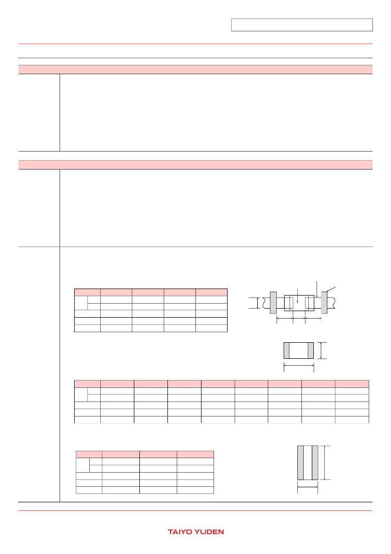
�The� following� diagrams� and� tables� show� some� examples� of� recommended� land� patterns� to� prevent� excessive� solder� amounts.�
�(1)Recommended� land� dimensions� for� typical� chip� capacitors�
�●Multilayer� Ceramic� Capacitors� :� Recommended� land� dimensions�
�(unit:� mm)�
�Land� patterns� for� PCBs�
�Land� pattern�
�Wave-soldering�
�Chip� capacitor�
�Solder-resist�
�Type�
�107�
�212�
�316�
�325�
�Size�
�L� 1.6� 2.0� 3.2� 3.2�
�W� 0.8� 1.25� 1.6� 2.5�
�A� 0.8� to� 1.0� 1.0� to� 1.4� 1.8� to� 2.5� 1.8� to� 2.5�
�B� 0.5� to� 0.8� 0.8� to� 1.5� 0.8� to� 1.7� 0.8� to� 1.7�
�C�
�B� A� B�
�C� 0.6� to� 0.8� 0.9� to� 1.2� 1.2� to� 1.6� 1.8� to� 2.5�
�Chip� capacitor�
�W�
�Technical�
�considerations�
�Reflow-soldering�
�L�
�Type�
�042�
�063�
�105�
�107�
�212�
�316�
�325�
�432�
�Size�
�L� 0.4� 0.6� 1.0�
�W� 0.2� 0.3� 0.5�
�A� 0.15� to� 0.25� 0.20� to� 0.30� 0.45� to� 0.55�
�B� 0.15� to� 0.20� 0.20� to� 0.30� 0.40� to� 0.50�
�C� 0.15� to� 0.30� 0.25� to� 0.40� 0.45� to� 0.55�
�1.6� 2.0� 3.2�
�0.8� 1.25� 1.6�
�0.8� to� 1.0� 0.8� to� 1.2� 1.8� to� 2.5�
�0.6� to� 0.8� 0.8� to� 1.2� 1.0� to� 1.5�
�0.6� to� 0.8� 0.9� to� 1.6� 1.2� to� 2.0�
�3.2�
�2.5�
�1.8� to� 2.5�
�1.0� to� 1.5�
�1.8� to� 3.2�
�4.5�
�3.2�
�2.5� to� 3.5�
�1.5� to� 1.8�
�2.3� to� 3.5�
�Note:Recommended� land� size� might� be� different� according�
�to� the� allowance� of� the� size� of� the� product.�
�●LWDC:� Recommended� land� dimensions� for� reflow-soldering�
�(unit:� mm)�
�LWDC�
�Type�
�105�
�107�
�212�
�Size�
�L� 0.52� 0.8� 1.25�
�W� 1.0� 1.6� 2.0�
�A� 0.18� to� 0.22� 0.25� to� 0.3� 0.5� to� 0.7�
�B� 0.2� to� 0.25� 0.3� to� 0.4� 0.4� to� 0.5�
�C� 0.9� to� 1.1� 1.5� to� 1.7� 1.9� to� 2.1�
�L�
�W�
�?� This� catalog� contains� the� typical� specification� only� due� to� the� limitation� of� space.� When� you� consider� the� purchase� of� our� products,� please� check� our� specification.�
�For� details� of� each� product� (characteristics� graph,� reliability� information,� precautions� for� use,� and� so� on),� see� our� Web� site� (http://www.ty-top.com/)� .�
�c_mlcc_prec_e-E02R01�
�相关PDF资料 |
PDF描述 |
|---|---|
| LTC4261CGN#TRPBF | IC CTRLR HOTSWAP W/ADC 28-SSOP |
| RSA32DTAI | CONN EDGECARD 64POS R/A .125 SLD |
| LTC4245IG#PBF | IC CNTRLR HOT SWAP 36-SSOP |
| TOP221YN | IC OFFLINE SWIT PWM OCP HV TO220 |
| ISPLSI 2032A-80LTN48 | IC PLD ISP 32I/O 15NS 48TQFP |
相关代理商/技术参数 |
参数描述 |
|---|---|
| LMK316BJ106ML-T | 功能描述:多层陶瓷电容器MLCC - SMD/SMT CAP MLCC 1206 10V X5R 10uF 20% RoHS:否 制造商:American Technical Ceramics (ATC) 电容:10 pF 容差:1 % 电压额定值:250 V 温度系数/代码:C0G (NP0) 外壳代码 - in:0505 外壳代码 - mm:1414 工作温度范围:- 55 C to + 125 C 产品:Low ESR MLCCs 封装:Reel |
| LMK316BJ225KL-T | 制造商:TAIYO YUDEN 功能描述:CAPACITOR, CERAMIC, MULTILAYER, 10 V, X7R, 2.2 UF, SURFACE MOUNT, 1206 |
| LMK316BJ225MD-T | 功能描述:多层陶瓷电容器MLCC - SMD/SMT CAP MLCC 1206 10V X5R 2.2uF 20% RoHS:否 制造商:American Technical Ceramics (ATC) 电容:10 pF 容差:1 % 电压额定值:250 V 温度系数/代码:C0G (NP0) 外壳代码 - in:0505 外壳代码 - mm:1414 工作温度范围:- 55 C to + 125 C 产品:Low ESR MLCCs 封装:Reel |
| LMK316BJ226KL-T | 功能描述:多层陶瓷电容器MLCC - SMD/SMT CAP MLCC 1206 10V X5R 22uF 10% RoHS:否 制造商:American Technical Ceramics (ATC) 电容:10 pF 容差:1 % 电压额定值:250 V 温度系数/代码:C0G (NP0) 外壳代码 - in:0505 外壳代码 - mm:1414 工作温度范围:- 55 C to + 125 C 产品:Low ESR MLCCs 封装:Reel |
| LMK316BJ226MD-T | 功能描述:多层陶瓷电容器MLCC - SMD/SMT CAP MLCC 1206 10V X5R 22uF 20% RoHS:否 制造商:American Technical Ceramics (ATC) 电容:10 pF 容差:1 % 电压额定值:250 V 温度系数/代码:C0G (NP0) 外壳代码 - in:0505 外壳代码 - mm:1414 工作温度范围:- 55 C to + 125 C 产品:Low ESR MLCCs 封装:Reel |
发布紧急采购,3分钟左右您将得到回复。