- 您现在的位置:买卖IC网 > PDF目录13768 > LMR10510XMFX/NOPB (National Semiconductor)IC REG BUCK ADJ 1A SOT23-5 PDF资料下载
参数资料
| 型号: | LMR10510XMFX/NOPB |
| 厂商: | National Semiconductor |
| 文件页数: | 10/26页 |
| 文件大小: | 0K |
| 描述: | IC REG BUCK ADJ 1A SOT23-5 |
| 标准包装: | 3,000 |
| 系列: | SIMPLE SWITCHER® |
| 类型: | 降压(降压) |
| 输出类型: | 可调式 |
| 输出数: | 1 |
| 输出电压: | 0.6 V ~ 4.5 V |
| 输入电压: | 3 V ~ 5.5 V |
| PWM 型: | 电流模式 |
| 频率 - 开关: | 1.6MHz |
| 电流 - 输出: | 1A |
| 同步整流器: | 无 |
| 工作温度: | -40°C ~ 125°C |
| 安装类型: | 表面贴装 |
| 封装/外壳: | SC-74A,SOT-753 |
| 包装: | 带卷 (TR) |
| 供应商设备封装: | SOT-23-5 |
�� ��
��
��SNVS727B� –� OCTOBER� 2011� –� REVISED� APRIL� 2013�
��Design� Guide�
�INDUCTOR� SELECTION�
�The� Duty� Cycle� (D)� can� be� approximated� quickly� using� the� ratio� of� output� voltage� (V� O� )� to� input� voltage� (V� IN� ):�
�D=�
�V� OUT�
�V� IN�
�The� catch� diode� (D1)� forward� voltage� drop� and� the� voltage� drop� across� the� internal� PMOS� must� be� included� to�
�calculate� a� more� accurate� duty� cycle.� Calculate� D� by� using� the� following� formula:�
�D=�
�V� OUT� +� V� D�
�V� IN� +� V� D� -� V� SW�
�V� SW� can� be� approximated� by:�
�V� SW� =� I� OUT� x� R� DSON�
�The� diode� forward� drop� (V� D� )� can� range� from� 0.3V� to� 0.7V� depending� on� the� quality� of� the� diode.� The� lower� the�
�V� D� ,� the� higher� the� operating� efficiency� of� the� converter.� The� inductor� value� determines� the� output� ripple� current.�
�Lower� inductor� values� decrease� the� size� of� the� inductor,� but� increase� the� output� ripple� current.� An� increase� in� the�
�inductor� value� will� decrease� the� output� ripple� current.�
�One� must� ensure� that� the� minimum� current� limit� (1.2A)� is� not� exceeded,� so� the� peak� current� in� the� inductor� must�
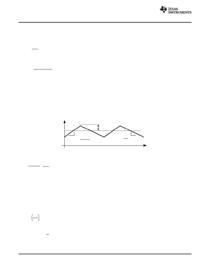
�be� calculated.� The� peak� current� (I� LPK� )� in� the� inductor� is� calculated� by:�
�I� LPK� =� I� OUT� +� Δ� i� L�
�'� i� L�
�I� OUT�
�V� IN� -� V� OUT�
�L�
�V� OUT�
�L�
�DT� S�
�T� S�
�t�
�Figure� 23.� Inductor� Current�
�V� IN� -� V� OUT�
�L�
�=�
�2� '� i� L�
�DT� S�
�In� general,�
�Δ� i� L� =� 0.1� x� (I� OUT� )� →� 0.2� x� (I� OUT� )�
�If� Δ� i� L� =� 20%� of� 1A,� the� peak� current� in� the� inductor� will� be� 1.2A.� The� minimum� specified� current� limit� over� all�
�operating� conditions� is� 1.2A.� One� can� either� reduce� Δ� i� L� ,� or� make� the� engineering� judgment� that� zero� margin� will�
�be� safe� enough.� The� typical� current� limit� is� 1.75A.�
�The� LMR10510� operates� at� frequencies� allowing� the� use� of� ceramic� output� capacitors� without� compromising�
�transient� response.� Ceramic� capacitors� allow� higher� inductor� ripple� without� significantly� increasing� output� ripple.�
�See� the� OUTPUT� CAPACITOR� section� for� more� details� on� calculating� output� voltage� ripple.� Now� that� the� ripple�
�current� is� determined,� the� inductance� is� calculated� by:�
�L=�
�DT� S�
�2� '� i� L�
�x� (V� IN� -� V� OUT� )�
�where�
�?�
�T� S� =�
�1�
�f� S�
�10�
��Product� Folder� Links:� LMR10510�
�Copyright� ?� 2011–2013,� Texas� Instruments� Incorporated�
�相关PDF资料 |
PDF描述 |
|---|---|
| HBC08DRAN-S734 | CONN EDGECARD 16POS .100 R/A PCB |
| LMR10510YSDX/NOPB | IC REG BUCK ADJ 1A 6LLP |
| HBC08DRAH-S734 | CONN EDGECARD 16POS .100 R/A PCB |
| GEC31DRYI-S734 | CONN EDGECARD 62POS DIP .100 SLD |
| GMC10DRXN-S734 | CONN EDGECARD 20POS DIP .100 SLD |
相关代理商/技术参数 |
参数描述 |
|---|---|
| LMR10510YMF/NOPB | 功能描述:直流/直流开关调节器 SIMPLE SWITCHER 5.5 Vin,1A SD Vltg Reg RoHS:否 制造商:International Rectifier 最大输入电压:21 V 开关频率:1.5 MHz 输出电压:0.5 V to 0.86 V 输出电流:4 A 输出端数量: 最大工作温度: 安装风格:SMD/SMT 封装 / 箱体:PQFN 4 x 5 |
| LMR10510YMFE/NOPB | 功能描述:直流/直流开关调节器 SIMPLE SWITCHER 5.5 Vin,1A SD Vltg Reg RoHS:否 制造商:International Rectifier 最大输入电压:21 V 开关频率:1.5 MHz 输出电压:0.5 V to 0.86 V 输出电流:4 A 输出端数量: 最大工作温度: 安装风格:SMD/SMT 封装 / 箱体:PQFN 4 x 5 |
| LMR10510YMFX/NOPB | 功能描述:直流/直流开关调节器 SIMPLE SWITCHER 5.5 Vin,1A SD Vltg Reg RoHS:否 制造商:International Rectifier 最大输入电压:21 V 开关频率:1.5 MHz 输出电压:0.5 V to 0.86 V 输出电流:4 A 输出端数量: 最大工作温度: 安装风格:SMD/SMT 封装 / 箱体:PQFN 4 x 5 |
| LMR10510YSD | 制造商:Texas Instruments 功能描述:BUCK, 1A, 5.5VIN 制造商:Texas Instruments 功能描述:BUCK, 1A, 5.5VIN; Primary Input Voltage:5.5V; No. of Outputs:1; Output Voltage:4.5V; Output Current:1A; Voltage Regulator Case Style:LLP; No. of Pins:6; Operating Temperature Min:-40C; Operating Temperature Max:125C; SVHC:No SVHC ;RoHS Compliant: Yes |
| LMR10510YSD/NOPB | 功能描述:直流/直流开关调节器 SIMPLE SWITCHER 5.5 Vin,1A SD Vltg Reg RoHS:否 制造商:International Rectifier 最大输入电压:21 V 开关频率:1.5 MHz 输出电压:0.5 V to 0.86 V 输出电流:4 A 输出端数量: 最大工作温度: 安装风格:SMD/SMT 封装 / 箱体:PQFN 4 x 5 |
发布紧急采购,3分钟左右您将得到回复。