- 您现在的位置:买卖IC网 > PDF目录17422 > LMR10510YSDDEMO/NOPB (National Semiconductor)BOARD EVAL FOR LMR10510 PDF资料下载
参数资料
| 型号: | LMR10510YSDDEMO/NOPB |
| 厂商: | National Semiconductor |
| 文件页数: | 15/26页 |
| 文件大小: | 0K |
| 描述: | BOARD EVAL FOR LMR10510 |
| 标准包装: | 1 |
| 系列: | SIMPLE SWITCHER® |
| 主要目的: | DC/DC,步降 |
| 输出及类型: | 1,非隔离 |
| 输出电压: | 1.8V |
| 电流 - 输出: | 1A |
| 输入电压: | 3 V ~ 5.5 V |
| 稳压器拓扑结构: | 降压 |
| 频率 - 开关: | 3MHz |
| 板类型: | 完全填充 |
| 已供物品: | 板 |
| 已用 IC / 零件: | LMR10510 |
�� ���
���
���SNVS727B� –� OCTOBER� 2011� –� REVISED� APRIL� 2013�
�The� first� step� is� to� determine� R� θ� JA� of� the� application.� The� LMR10510� has� over-temperature� protection� circuitry.�
�When� the� silicon� temperature� reaches� 165°C,� the� device� stops� switching.� The� protection� circuitry� has� a�
�hysteresis� of� about� 15°C.� Once� the� silicon� temperature� has� decreased� to� approximately� 150°C,� the� device� will�
�start� to� switch� again.� Knowing� this,� the� R� θ� JA� for� any� application� can� be� characterized� during� the� early� stages� of�
�the� design� one� may� calculate� the� R� θ� JA� by� placing� the� PCB� circuit� into� a� thermal� chamber.� Raise� the� ambient�
�temperature� in� the� given� working� application� until� the� circuit� enters� thermal� shutdown.� If� the� SW-pin� is� monitored,�
�it� will� be� obvious� when� the� internal� PFET� stops� switching,� indicating� a� junction� temperature� of� 165°C.� Knowing�
�the� internal� power� dissipation� from� the� above� methods,� the� junction� temperature,� and� the� ambient� temperature�
�R� θ� JA� can� be� determined.�
�R� T� JA� =�
�165° - Ta�
�P� INTERNAL�
�Once� this� is� determined,� the� maximum� ambient� temperature� allowed� for� a� desired� junction� temperature� can� be�
�found.�
�An� example� of� calculating� R� θ� JA� for� an� application� using� the� LMR10510� is� shown� below.�
�A� sample� PCB� is� placed� in� an� oven� with� no� forced� airflow.� The� ambient� temperature� was� raised� to� 147°C,� and� at�
�that� temperature,� the� device� went� into� thermal� shutdown.�
�From� the� previous� example:�
�P� INTERNAL� =� 149� mW�
�R� T� JA� =�
�165°C� -� 147°C�
�149� mW�
�=� 121°C/W�
�Since� the� junction� temperature� must� be� kept� below� 125°C,� then� the� maximum� ambient� temperature� can� be�
�calculated� as:�
�T� j� -� (R� θ� JA� x� P� LOSS� )� =� T� A�
�125°C� -� (121°C/W� x� 149� mW)� =� 107°C�
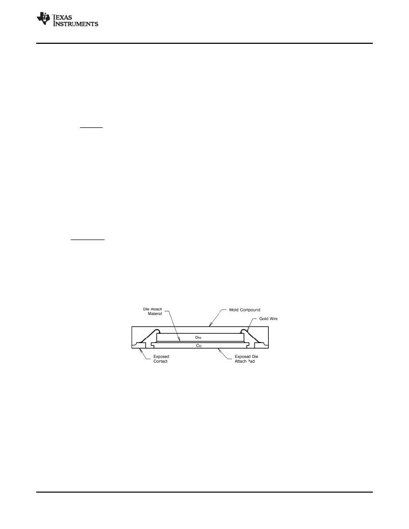
�WSON� Package�
�Figure� 24.� Internal� WSON� Connection�
�For� certain� high� power� applications,� the� PCB� land� may� be� modified� to� a� "dog� bone"� shape� (see� Figure� 25� ).� By�
�increasing� the� size� of� ground� plane,� and� adding� thermal� vias,� the� R� θ� JA� for� the� application� can� be� reduced.�
�Copyright� ?� 2011–2013,� Texas� Instruments� Incorporated�
�Product� Folder� Links:� LMR10510�
��15�
�相关PDF资料 |
PDF描述 |
|---|---|
| MIC2545A-1YTS TR | IC SW CURR LIMIT HI SIDE 14TSSOP |
| MIC2547-2YM TR | IC SW CURR LIMIT DUAL 16-SOP |
| GCM06DRSH-S288 | CONN EDGECARD 12POS .156 EXTEND |
| M7LTK-2410K | IDC CABLE - MDH24K/MC26F/MDL24K |
| GCM06DRSD-S288 | CONN EDGECARD 12POS .156 EXTEND |
相关代理商/技术参数 |
参数描述 |
|---|---|
| LMR10510YSDE/NOPB | 功能描述:直流/直流开关调节器 SIMPLE SWITCHER 5.5 Vin,1A SD Vltg Reg RoHS:否 制造商:International Rectifier 最大输入电压:21 V 开关频率:1.5 MHz 输出电压:0.5 V to 0.86 V 输出电流:4 A 输出端数量: 最大工作温度: 安装风格:SMD/SMT 封装 / 箱体:PQFN 4 x 5 |
| LMR10510YSDX | 制造商:TI 制造商全称:Texas Instruments 功能描述:SIMPLE SWITCHER?? 5.5Vin, 1A Step-Down Voltage Regulator in SOT-23 and LLP |
| LMR10510YSDX/NOPB | 功能描述:直流/直流开关调节器 SIMPLE SWITCHER 5.5 Vin,1A SD Vltg Reg RoHS:否 制造商:International Rectifier 最大输入电压:21 V 开关频率:1.5 MHz 输出电压:0.5 V to 0.86 V 输出电流:4 A 输出端数量: 最大工作温度: 安装风格:SMD/SMT 封装 / 箱体:PQFN 4 x 5 |
| LMR10515 | 制造商:TI 制造商全称:Texas Instruments 功能描述:SIMPLE SWITCHER? 5.5Vin, 1.5A Step-Down Voltage Regulator in SOT-23 and LLP |
| LMR10515XMF | 制造商:Texas Instruments 功能描述:BUCK, 1.5A, 5.5VIN 制造商:Texas Instruments 功能描述:BUCK, 1.5A, 5.5VIN; Primary Input Voltage:5.5V; No. of Outputs:1; Output Voltage:4.5V; Output Current:1.5A; Voltage Regulator Case Style:SOT-23; No. of Pins:5; Operating Temperature Min:-40C; Operating Temperature Max:125C; SVHC:No;RoHS Compliant: Yes |
发布紧急采购,3分钟左右您将得到回复。