- 您现在的位置:买卖IC网 > PDF目录358884 > LMV232TL (NATIONAL SEMICONDUCTOR CORP) Dual-Channel Integrated Mean Square Power Detector for CDMA & WCDMA PDF资料下载
参数资料
| 型号: | LMV232TL |
| 厂商: | NATIONAL SEMICONDUCTOR CORP |
| 元件分类: | 衰减器 |
| 英文描述: | Dual-Channel Integrated Mean Square Power Detector for CDMA & WCDMA |
| 中文描述: | 50 MHz - 2000 MHz RF/MICROWAVE LINEAR DETECTOR |
| 封装: | 1.50 X 1.50 MM, 0.60 MM HEIGHT, LEAD FREE, MO-211DD, MICRO SMD, 8 PIN |
| 文件页数: | 10/13页 |
| 文件大小: | 779K |
| 代理商: | LMV232TL |
Application Notes
(Continued)
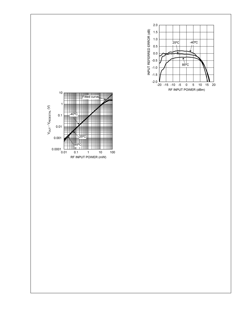
The detection curves of
Figure 2
show the detector response
to RF input power. To show the complete dynamic range on
a logarithmic scale, the pedestal voltage (V
PEDESTAL
) is sub-
tracted from the output. The pedestal voltage is defined as
the output voltage in the absence of an RF input signal (at
25C). The best-fit ideal mean square response is repre-
sented by the fitted curve in
Figure 2
. The input referred error
of the detection curves with respect to this best-fit mean
square response is determined as follows:
Determine the best-fit mean square response.
Determine the output referred error between the actual
detector response and the ideal mean square response.
Translate the output referred error to an input referred
error.
The best-fit linear curve is obtained from the detector re-
sponse by means of linear regression. The output referred
error is calculated with the formula:
Error
dBV
= 20*log[ (V
OUT
-V
PEDESTAL
)/(K
DET
*P
IN
) ]
Where,
Conversion gain of the ideal fitted curve K
DET
is in V/mW
and the RF input power P
IN
in mW.
To translate this output referred error (in dB) to an input
referred error, it has to be divided by a factor of 2. This is due
to the mean square characteristic of the device. The re-
sponse of a mean square detector changes by 2 dB for every
dB change of the input power.
Figure 3
depicts the resulting
curve.
Analyzing
Figure 3
shows that three sections can be distin-
guished:
At higher power levels the error increases.
A middle section where the error is constant and rela-
tively small.
At lower power levels the error increases again.
These three sections are leading back to three error mecha-
nisms. At higher power levels the detectors output starts to
saturate because the output voltage approaches the maxi-
mum signal swing that the detector can handle. The maxi-
mum output voltage of the device thus limits the upper end of
the detection range.Also the maximum allowedADC voltage
of the baseband chip can limit the detection range at higher
power levels. By adjusting the feedback resistor R
of
Figure 1
the upper end of the range can be shifted. This is
valid until the detector cell inside the LMV232 is the limiting
factor.
The middle section of the error curve shows a small error
variation. This is the section where the detector is used and
is called the detection range of the detector. This range is
limited on both sides by a maximum allowed error.
For low input power levels, the variation of output voltage is
very small. Therefore the measurement resolution ADC is
important in order to measure those small variations. Offsets
and temperature variation impact the accuracy at low power
levels as well.
DETECTION ERROR OVER TEMPERATURE
Like any power detector device, the output signal of the
LMV232 mean square power detector shows some residual
variation over temperature that limits it’s dynamic range. The
variation determines the accuracy and range of input power
levels for which the detector produces an accurate output
signal.
The error over temperature is mainly caused by the variation
of the pedestal voltage. Besides this, a minimal error contri-
bution leads back to the conversion gain variation of the
detector. This conversion gain error is visible in the mid-
power range, where the temperature error curves of
Figure 3
run parallel to each other. Since the conversion gain varia-
tion is acceptable, the focus will be on the pedestal voltage
variation over temperature.
20127884
FIGURE 2. Detection Curve
20127869
FIGURE 3. Input referred Error vs. RF Input Power
L
www.national.com
10
相关PDF资料 |
PDF描述 |
|---|---|
| LMV232TLX | Dual-Channel Integrated Mean Square Power Detector for CDMA & WCDMA |
| LMV242MDA | MICA RoHS Compliant: No |
| LMV242LD | Dual Output, Quad-Band GSM/GPRS Power Amplifier Controller |
| LMV242MWA | Dual Output, Quad-Band GSM/GPRS Power Amplifier Controller |
| LMV242LDX | Silver Mica Capacitor; Capacitance:510pF; Capacitance Tolerance: 5%; Series:CDV30; Voltage Rating:1500VDC; Capacitor Dielectric Material:Mica; Termination:Radial Leaded; Lead Pitch:11.1mm; Leaded Process Compatible:No RoHS Compliant: No |
相关代理商/技术参数 |
参数描述 |
|---|---|
| LMV232TL/NOPB | 功能描述:射频检测器 RoHS:否 制造商:Skyworks Solutions, Inc. 配置: 频率范围:650 MHz to 3 GHz 最大二极管电容: 最大工作温度:+ 85 C 最小工作温度:- 40 C 封装 / 箱体:SC-88 封装:Reel |
| LMV232TLEVAL | 功能描述:射频开发工具 LMV232TL EVAL BOARD RoHS:否 制造商:Taiyo Yuden 产品:Wireless Modules 类型:Wireless Audio 工具用于评估:WYSAAVDX7 频率: 工作电源电压:3.4 V to 5.5 V |
| LMV232TLX | 制造商:NSC 制造商全称:National Semiconductor 功能描述:Dual-Channel Integrated Mean Square Power Detector for CDMA & WCDMA |
| LMV232TLX/NOPB | 功能描述:射频检测器 RoHS:否 制造商:Skyworks Solutions, Inc. 配置: 频率范围:650 MHz to 3 GHz 最大二极管电容: 最大工作温度:+ 85 C 最小工作温度:- 40 C 封装 / 箱体:SC-88 封装:Reel |
| LMV241C WAF | 制造商:Texas Instruments 功能描述: |
发布紧急采购,3分钟左右您将得到回复。