- 您现在的位置:买卖IC网 > PDF目录358886 > LMX1501AMX (NATIONAL SEMICONDUCTOR CORP) PLLatinumTM 1.1 GHz Frequency Synthesizer for RF Personal Communications PDF资料下载
参数资料
| 型号: | LMX1501AMX |
| 厂商: | NATIONAL SEMICONDUCTOR CORP |
| 元件分类: | XO, clock |
| 英文描述: | PLLatinumTM 1.1 GHz Frequency Synthesizer for RF Personal Communications |
| 中文描述: | PLL FREQUENCY SYNTHESIZER, 1100 MHz, PDSO16 |
| 封装: | 0.150 INCH, PLASTIC, SOP-16 |
| 文件页数: | 2/22页 |
| 文件大小: | 367K |
| 代理商: | LMX1501AMX |
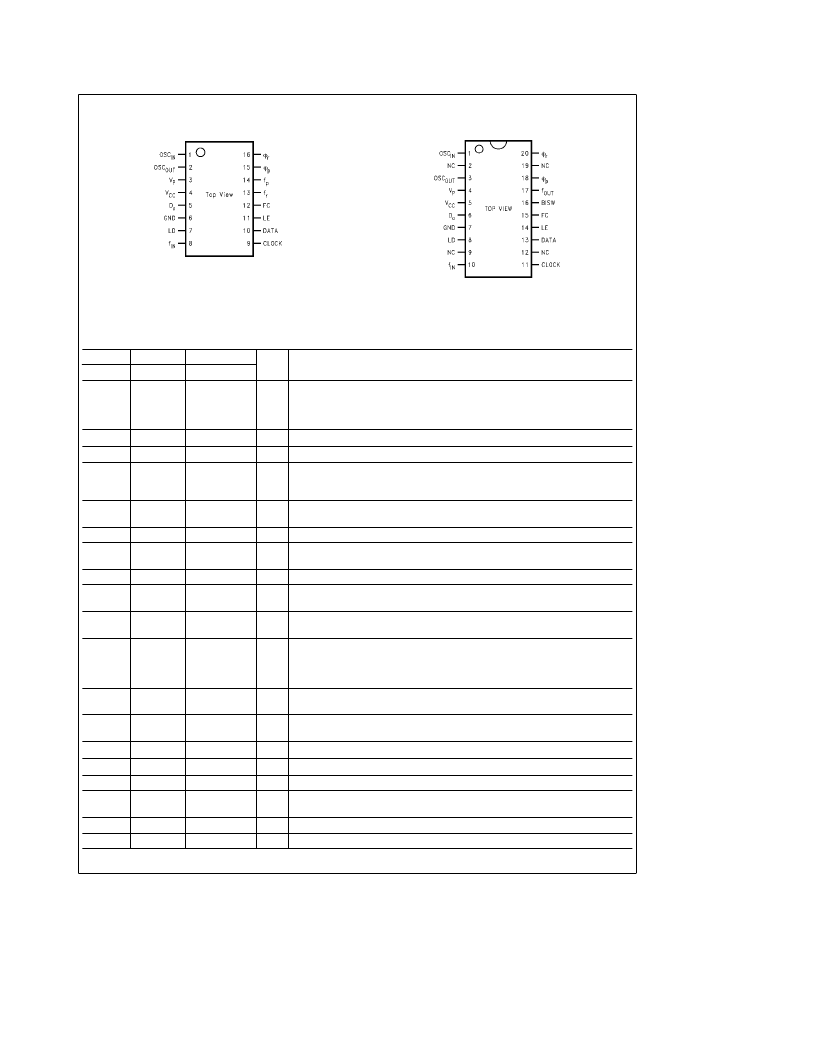
Connection Diagrams
LMX1501A
TL/W/12340–2
JEDEC 16-Lead (0.150
×
Wide) Small
Outline Molded Package (M)
Order Number LMX1501AM or LMX1501AMX
See NS Package Number M16A
LMX1511
TL/W/12340–3
20-Lead (0.173
×
Wide) Thin Shrink
Small Outline Package (TM)
Order Number LMX1511TM or LMX1511TMX
See NS Package Number MTC20
Pin Descriptions
Pin No.
Pin No.
Pin Name
I/O
Description
1501A
1511
1501A/1511
1
1
OSC
IN
I
Oscillator input. A CMOS inverting gate input intended for connection to a
crystal resonator for operation as an oscillator. The input has a V
CC
/2 input
threshold and can be driven from an external CMOS or TTL logic gate. May also
be used as a buffer for an externally provided reference oscillator.
2
3
OSC
OUT
O
Oscillator output.
3
4
V
P
Power supply for charge pump must be
t
V
CC
.
4
5
V
CC
Power supply voltage input. Input may range from 2.7V to 5.5V. Bypass
capacitors should be placed as close as possible to this pin and be connected
directly to the ground plane.
5
6
D
o
O
Internal charge pump output. For connection to a loop filter for driving the input
of an external VCO.
6
7
GND
Ground.
7
8
LD
O
Lock detect. Output provided to indicate when the VCO frequency is in ‘‘lock’’.
When the loop is locked, the pin’s output is HIGH with narrow low pulses.
8
10
f
IN
I
Prescaler input. Small signal input from the VCO.
9
11
CLOCK
I
High impedance CMOS Clock input. Data is clocked in on the rising edge, into
the various counters and registers.
10
13
DATA
I
Binary serial data input. Data entered MSB first. LSB is control bit. High
impedance CMOS input.
11
14
LE
I
Load enable input (with internal pull-up resistor). When LE transitions HIGH,
data stored in the shift registers is loaded into the appropriate latch (control bit
dependent). Clock must be low when LE toggles high or low. See Serial Data
Input Timing Diagram.
12
15
FC
I
Phase control select (with internal pull-up resistor). When FC is LOW, the
polarity of the phase comparator and charge pump combination is reversed.
X
16
BISW
O
Analog switch output. When LE is HIGH, the analog switch is ON, routing the
internal charge pump output through BISW (as well as through D
o
).
13
f
r
O
Monitor pin of phase comparator input. Programmable reference divider output.
14
f
p
O
Monitor pin of phase comparator input. Programmable divider output.
X
17
f
OUT
O
Monitor pin of phase comparator input. CMOS Output.
15
18
w
p
O
Output for external charge pump.
w
p
is an open drain N-channel transistor and
requires a pull-up resistor.
16
20
w
r
O
Output for external charge pump.
w
r
is a CMOS logic output.
X
2,9,12,19
NC
No connect.
2
相关PDF资料 |
PDF描述 |
|---|---|
| LMX15010AM | 1.1 GHz Frequency Synthesizer for RF Personal Communications(367.82 k) |
| LMX1600SLB | PLLatinum⑩ Low Cost Dual Frequency Synthesizer |
| LMX1600TM | PLLatinum⑩ Low Cost Dual Frequency Synthesizer |
| LMX2312USLDX | PLLatinum⑩ Ultra Low Power Frequency Synthesizer for RF Personal Communications |
| LMX2312U | PLLatinum⑩ Ultra Low Power Frequency Synthesizer for RF Personal Communications |
相关代理商/技术参数 |
参数描述 |
|---|---|
| LMX1511 | 制造商:NSC 制造商全称:National Semiconductor 功能描述:PLLatinumTM 1.1 GHz Frequency Synthesizer for RF Personal Communications |
| LMX1511TM | 制造商:NSC 制造商全称:National Semiconductor 功能描述:PLLatinumTM 1.1 GHz Frequency Synthesizer for RF Personal Communications |
| LMX1511TMX | 功能描述:IC FREQ SYNTHESZR 1.1GHZ 20TSSOP RoHS:否 类别:集成电路 (IC) >> 时钟/计时 - 时钟发生器,PLL,频率合成器 系列:PLLatinum™ 标准包装:39 系列:- 类型:* PLL:带旁路 输入:时钟 输出:时钟 电路数:1 比率 - 输入:输出:1:10 差分 - 输入:输出:是/是 频率 - 最大:170MHz 除法器/乘法器:无/无 电源电压:2.375 V ~ 3.465 V 工作温度:0°C ~ 70°C 安装类型:* 封装/外壳:* 供应商设备封装:* 包装:* |
| LMX1531LQ1515E | 制造商:NSC 制造商全称:National Semiconductor 功能描述:High Performance Frequency Synthesizer System with Integrated VCO |
| LMX156 | 制造商:未知厂家 制造商全称:未知厂家 功能描述:Analog IC |
发布紧急采购,3分钟左右您将得到回复。