- 您现在的位置:买卖IC网 > PDF目录98001 > LMX2316MWC (NATIONAL SEMICONDUCTOR CORP) PLL FREQUENCY SYNTHESIZER, 1200 MHz, UUC PDF资料下载
参数资料
| 型号: | LMX2316MWC |
| 厂商: | NATIONAL SEMICONDUCTOR CORP |
| 元件分类: | PLL合成/DDS/VCOs |
| 英文描述: | PLL FREQUENCY SYNTHESIZER, 1200 MHz, UUC |
| 封装: | WAFER |
| 文件页数: | 12/22页 |
| 文件大小: | 305K |
| 代理商: | LMX2316MWC |
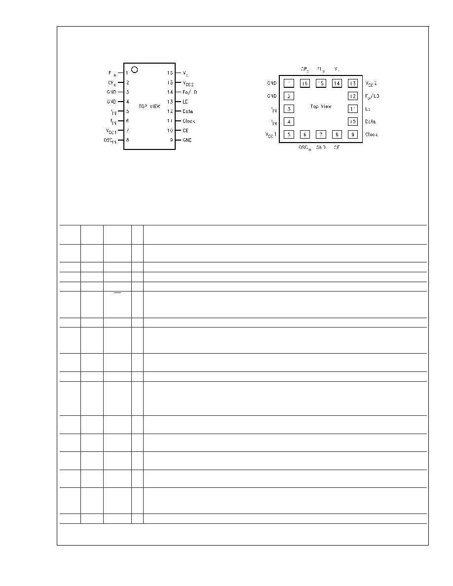
Connection Diagrams
Pin Descriptions
16-Pin
TSSOP
16-Pin
CSP
Pin
Name
I/O
Description
115
FL
o
O
FastLock Output. For connection of parallel resistor to the loop filter. (See Section 1.3.4
FASTLOCK MODES description.)
216
CP
o
O
Charge Pump Output. For connection to a loop filter for driving the input of an external VCO.
3
1
GND
Charge Pump Ground.
4
2
GND
Analog Ground.
53
f
IN
I
RF Prescaler Complementary Input. A bypass capacitor should be placed as close as possible to
this pin and be connected directly to the ground plane. The complementary input can be left
unbypassed, with some degradation in RF sensitivity.
64
f
IN
I
RF Prescaler Input. Small signal input from the VCO.
75
V
CC1
Analog Power Supply Voltage Input. Input may range from 2.3V to 5.5V. Bypass capacitors should
be placed as close as possible to this pin and be connected directly to the ground plane. V
CC1
must equal V
CC2.
8
6
OSC
IN
I
Oscillator Input. This input is a CMOS input with a threshold of approximately V
CC/2 and an
equivalent 100k input resistance. The oscillator input is driven from a reference oscillator.
9
7
GND
Digital Ground.
10
8
CE
I
Chip Enable. A LOW on CE powers down the device and will TRI-STATE the charge pump output.
Taking CE HIGH will power up the device depending on the status of the power down bit F2. (See
Section 1.3.1 POWERDOWN OPERATION and Section 1.7.1 DEVICE PROGRAMMING AFTER
FIRST APPLYING V
CC.)
11
9
Clock
I
High Impedance CMOS Clock Input. Data for the various counters is clocked in on the rising edge
into the 21-bit shift register.
12
10
Data
I
Binary Serial Data Input. Data entered MSB first. The last two bits are the control bits. High
impedance CMOS input.
13
11
LE
I
Load Enable CMOS Input. When LE goes HIGH, data stored in the shift registers is loaded into one
of the 3 appropriate latches (control bit dependent).
14
12
Fo/LD
O
Multiplexed Output of the RF Programmable or Reference Dividers and Lock Detect. CMOS output.
(See
Table 4.)
15
13
V
CC2
Digital Power Supply Voltage Input. Input may range from 2.3V to 5.5V. Bypass capacitors should
be placed as close as possible to this pin and be connected directly to the ground plane. V
CC1
must equal V
CC2.
16
14
V
P
Power Supply for Charge Pump. Must be
≥ V
CC.
LMX2306/16/26
DS100127-2
16-Lead (0.173” Wide) Thin Shrink Small Outline
Package(TM)
Order Number LMX2306TM, LMX2306TMX,
LMX2316TM, LMX2316TMX,
LMX2326TM or LMX2326TMX
See NS Package Number MTC16
LMX2306/16/26
DS100127-19
16-pin Chip Scale Package
Order Number LMX2306SLBX, LMX2316SLBX or
LM2326SLBX
See NS Package Number SLB16A
LMX2306/LMX2316/LMX2326
www.national.com
2
相关PDF资料 |
PDF描述 |
|---|---|
| LMX2316SLB | PLL FREQUENCY SYNTHESIZER, 1200 MHz, CQCC16 |
| LMX2321TMX | PLL FREQUENCY SYNTHESIZER, 2100 MHz, PDSO16 |
| LMX2324ATM | PLL FREQUENCY SYNTHESIZER, 2200 MHz, PDSO16 |
| LMX2364TMX/NOPB | PLL FREQUENCY SYNTHESIZER, 2600 MHz, PDSO24 |
| LMX2372MDC | PLL FREQUENCY SYNTHESIZER, 1200 MHz, UUC |
相关代理商/技术参数 |
参数描述 |
|---|---|
| LMX2316SLBX | 制造商:NSC 制造商全称:National Semiconductor 功能描述:PLLatinum⑩ Low Power Frequency Synthesizer for RF Personal Communications |
| LMX2316SLBX/NOPB | 功能描述:IC FREQ SYNTH 1.2GHZ 16LAMIN CSP RoHS:是 类别:集成电路 (IC) >> 时钟/计时 - 时钟发生器,PLL,频率合成器 系列:PLLatinum™ 标准包装:39 系列:- 类型:* PLL:带旁路 输入:时钟 输出:时钟 电路数:1 比率 - 输入:输出:1:10 差分 - 输入:输出:是/是 频率 - 最大:170MHz 除法器/乘法器:无/无 电源电压:2.375 V ~ 3.465 V 工作温度:0°C ~ 70°C 安装类型:* 封装/外壳:* 供应商设备封装:* 包装:* |
| LMX2316TM | 制造商:Texas Instruments 功能描述:PLL Frequency Synthesizer Single 100MHz to 1200MHz 16-Pin TSSOP Rail |
| LMX2316TM | 制造商:Texas Instruments 功能描述:1.2GHZ SINGLE PLL 2316 TSSOP16 |
| LMX2316TM/NOPB | 功能描述:IC FREQ SYNTHESIZER 16-TSSOP RoHS:是 类别:集成电路 (IC) >> 时钟/计时 - 时钟发生器,PLL,频率合成器 系列:PLLatinum™ 标准包装:39 系列:- 类型:* PLL:带旁路 输入:时钟 输出:时钟 电路数:1 比率 - 输入:输出:1:10 差分 - 输入:输出:是/是 频率 - 最大:170MHz 除法器/乘法器:无/无 电源电压:2.375 V ~ 3.465 V 工作温度:0°C ~ 70°C 安装类型:* 封装/外壳:* 供应商设备封装:* 包装:* |
发布紧急采购,3分钟左右您将得到回复。