- 您现在的位置:买卖IC网 > PDF目录44573 > LMX2330LMDC (NATIONAL SEMICONDUCTOR CORP) PLL FREQUENCY SYNTHESIZER, 2500 MHz, UUC PDF资料下载
参数资料
| 型号: | LMX2330LMDC |
| 厂商: | NATIONAL SEMICONDUCTOR CORP |
| 元件分类: | PLL合成/DDS/VCOs |
| 英文描述: | PLL FREQUENCY SYNTHESIZER, 2500 MHz, UUC |
| 封装: | DIE |
| 文件页数: | 20/26页 |
| 文件大小: | 631K |
| 代理商: | LMX2330LMDC |
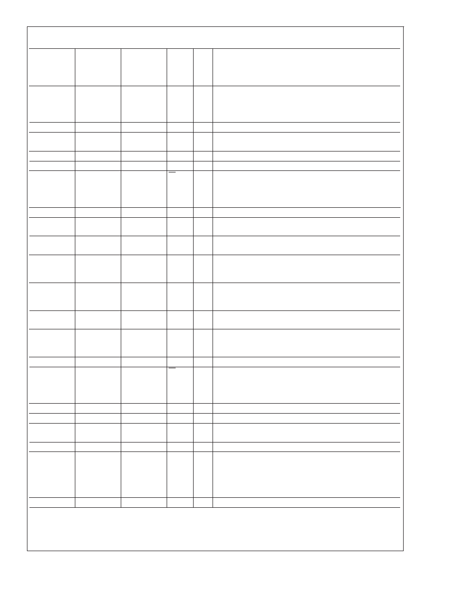
Pin Descriptions
Pin No.
LMX233XLSLD
20-pin Thin
CSP Package
Pin No.
LMX233XLSLB
24-pin CSP
Package
Pin No.
LMX233XLTM
20-pin TSSOP
Package
Pin
Name
I/O
Description
20
24
1
V
CC1
—
Power supply voltage input for RF analog and RF digital circuits.
Input may range from 2.7V to 5.5V. V
CC1 must equal VCC2.
Bypass capacitors should be placed as close as possible to this
pin and be connected directly to the ground plane.
122
V
P1
—
Power Supply for RF charge pump. Must be
≥ V
CC.
233
D
o RF
O
Internal charge pump output. For connection to a loop filter for
driving the input of an external VCO.
3
4
GND
—
Ground for RF digital circuitry.
455
f
IN RF
I
RF prescaler input. Small signal input from the VCO.
566
f
IN RF
I
RF prescaler complementary input. A bypass capacitor should
be placed as close as possible to this pin and be connected
directly to the ground plane. Capacitor is optional with some loss
of sensitivity.
6
7
GND
—
Ground for RF analog circuitry.
788
OSC
in
I
Oscillator input. The input has a V
CC/2 input threshold and can
be driven from an external CMOS or TTL logic gate.
8
10
9
GND
—
Ground for IF digital, MICROWIRE,F
oLD, and oscillator
circuits.
911
10
F
oLD
O
Multiplexed output of the RF/IF programmable or reference
dividers, RF/IF lock detect signals and Fastlock mode. CMOS
output
(see Programmable Modes).
10
12
11
Clock
I
High impedance CMOS Clock input. Data for the various
counters is clocked in on the rising edge, into the 22-bit shift
register.
11
14
12
Data
I
Binary serial data input. Data entered MSB first. The last two bits
are the control bits. High impedance CMOS input.
12
15
13
LE
I
Load enable high impedance CMOS input. When LE goes HIGH,
data stored in the shift registers is loaded into one of the 4
appropriate latches (control bit dependent).
13
16
14
GND
—
Ground for IF analog circuitry.
14
17
15
f
IN IF
I
IF prescaler complementary input. A bypass capacitor should be
placed as close as possible to this pin and be connected directly
to the ground plane. Capacitor is optional with some loss of
sensitivity.
15
18
16
f
IN RF
I
IF prescaler input. Small signal input from the VCO.
16
19
17
GND
—
Ground for IF digital, MICROWIRE, F
oLD, and oscillator circuits.
17
20
18
D
o IF
O
IF charge pump output. For connection to a loop filter for driving
the input of an external VCO.
18
22
19
V
P2
—
Power Supply for IF charge pump. Must be
≥ V
CC.
19
23
20
V
CC2
—
Power supply voltage input for IF analog, IF digital,
MICROWIRE, F
oLD, and oscillator circuits. Input may range from
2.7V to 5.5V. V
CC2 must equal VCC1. Bypass capacitors should
be placed as close as possible to this pin and be connected
directly to the ground plane.
X
1, 9, 13, 21
X
NC
—
No connect.
LMX2330L/LMX2331L/LMX2332L
www.national.com
3
相关PDF资料 |
PDF描述 |
|---|---|
| LMX2330LTM/NOPB | PLL FREQUENCY SYNTHESIZER, 2500 MHz, PDSO20 |
| LMX2331LTMX/NOPB | PLL FREQUENCY SYNTHESIZER, 2000 MHz, PDSO20 |
| LMX2332LTM/NOPB | PLL FREQUENCY SYNTHESIZER, 1200 MHz, PDSO20 |
| LMX2331LTM/NOPB | PLL FREQUENCY SYNTHESIZER, 2000 MHz, PDSO20 |
| LMX2331LMDA | PLL FREQUENCY SYNTHESIZER, 2000 MHz, UUC |
相关代理商/技术参数 |
参数描述 |
|---|---|
| LMX2330LSBX | 制造商:NSC 制造商全称:National Semiconductor 功能描述:PLLatinumTM Low Power Dual Frequency Synthesizer for RF Personal Communications |
| LMX2330LSLB | 制造商:NSC 制造商全称:National Semiconductor 功能描述:PLLatinum⑩ Low Power Dual Frequency Synthesizer for RF Personal Communications |
| LMX2330LSLBX | 制造商:未知厂家 制造商全称:未知厂家 功能描述:Serial-Input Frequency Synthesizer |
| LMX2330LSLBX/NOPB | 功能描述:IC FREQ SYNTH DUAL 24LAMINATECSP RoHS:是 类别:集成电路 (IC) >> 时钟/计时 - 时钟发生器,PLL,频率合成器 系列:PLLatinum™ 标准包装:39 系列:- 类型:* PLL:带旁路 输入:时钟 输出:时钟 电路数:1 比率 - 输入:输出:1:10 差分 - 输入:输出:是/是 频率 - 最大:170MHz 除法器/乘法器:无/无 电源电压:2.375 V ~ 3.465 V 工作温度:0°C ~ 70°C 安装类型:* 封装/外壳:* 供应商设备封装:* 包装:* |
| LMX2330LSLDX | 制造商:NSC 制造商全称:National Semiconductor 功能描述:PLLatinumTM Low Power Dual Frequency Synthesizer for RF Personal Communications |
发布紧急采购,3分钟左右您将得到回复。