- 您现在的位置:买卖IC网 > PDF目录19798 > LNK586DG-TL (Power Integrations)IC OFFLINE SW SO8C PDF资料下载
参数资料
| 型号: | LNK586DG-TL |
| 厂商: | Power Integrations |
| 文件页数: | 6/16页 |
| 文件大小: | 0K |
| 描述: | IC OFFLINE SW SO8C |
| 产品培训模块: | LinkZero-AX |
| 标准包装: | 2,500 |
| 系列: | LinkZero™-AX |
| 输出隔离: | 任意一种 |
| 频率范围: | 93kHz ~ 107kHz |
| 输入电压: | 85 ~ 265VAC |
| 输出电压: | 700V |
| 功率(瓦特): | 6W |
| 工作温度: | -40°C ~ 125°C |
| 封装/外壳: | 8-SOIC(0.154",3.90mm 宽)7 引线 |
| 供应商设备封装: | SO-8C |
| 包装: | 带卷 (TR) |
�� �
�
�LNK584-586�
�C� B�
�D� B�
�R� S�
�C� S�
�D� BP�
�R� BP�
�D� O�
�R� FB2�
�C� FB�
�C� BP�
�R� FB1�
�Transformer�
�R6�
�C� O�
�U1�
�J3�
�IN�
�DC�
�T1�
�PI-6098-082310�
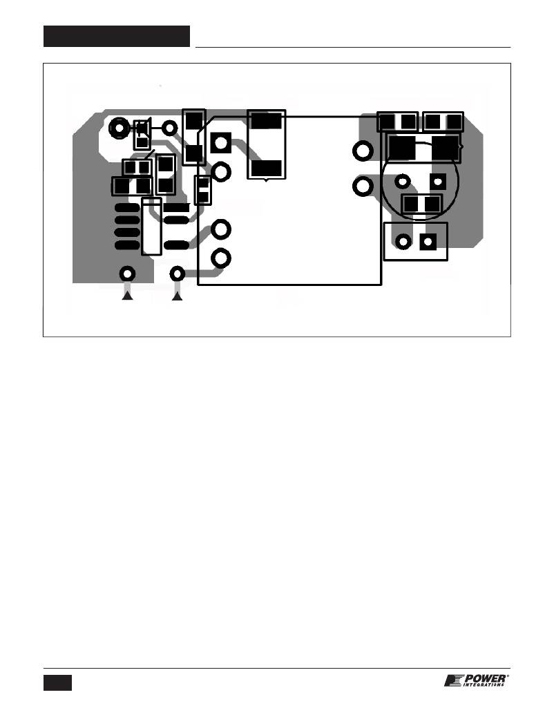
�Figure� 5.�
�PCB� Layout� of� a� 2.1� W,� 6� V,� 350� mA� Charger.�
�Output� Diode� (D� O� )�
�For� best� performance,� the� area� of� the� loop� connecting� the�
�secondary� winding,� the� output� diode� (D� O� )� and� the� output� filter�
�capacitor� (C� O� )� should� be� minimized.� In� addition,� sufficient�
�copper� area� should� be� provided� at� the� anode� and� cathode�
�terminals� of� the� diode� for� heat� sinking.� A� larger� area� is� preferred�
�at� the� electrically� “quiet”� cathode� terminal.� A� large� anode� area�
�can� increase� high� frequency� conducted� and� radiated� EMI.�
�Resistor� R� S� and� C� S� represent� the� secondary� side� RC� snubber.�
�Quick� Design� Checklist�
�As� with� any� power� supply� design,� all� LinkZero-AX� designs�
�should� be� verified� on� the� bench� to� make� sure� that� component�
�specifications� are� not� exceeded� under� worst-case� conditions.�
�The� following� minimum� set� of� tests� is� strongly� recommended:�
�1.� Maximum� drain� voltage� –� Verify� that� V� DS� does� not� exceed�
�660� V� at� the� highest� input� voltage� and� peak� (overload)� output�
�power.� This� margin� to� the� 700� V� BV� DSS� specification� gives�
�margin� for� design� variation,� especially� in� clampless� designs.�
�6�
�Rev.� B� 11/12�
�2.� Maximum� drain� current� –� At� maximum� ambient� temperature,�
�maximum� input� voltage� and� peak� output� (overload)� power,�
�verify� drain� current� waveforms� for� any� signs� of� transformer�
�saturation� and� excessive� leading-edge� current� spikes� at�
�start-up.� Repeat� under� steady� state� conditions� and� verify�
�that� the� leading-edge� current� spike� event� is� below� I� LIMIT(MIN)� at�
�the� end� of� the� t� LEB(MIN)� .� Under� all� conditions,� the� maximum�
�drain� current� should� be� below� the� specified� absolute�
�maximum� ratings.�
�3.� Thermal� check� –� At� specified� maximum� output� power,�
�minimum� input� voltage� and� maximum� ambient� temperature,�
�verify� that� the� temperature� specifications� are� not� exceeded�
�for� LinkZero-AX,� transformer,� output� diode� and� output�
�capacitors.� Enough� thermal� margin� should� be� allowed� for�
�part-to-part� variation� of� the� R� DS(ON)� of� LinkZero-AX� as� specified�
�in� the� data� sheet.� Under� low� line� and� maximum� power,� maxi-�
�mum� LinkZero-AX� source� pin� temperature� of� 100� °C� is�
�recommended� to� allow� for� these� variations.�
�www.powerint.com�
�相关PDF资料 |
PDF描述 |
|---|---|
| GEC08DREN-S734 | CONN EDGECARD 16POS .100 EYELET |
| GSM36DTMD-S273 | CONN EDGECARD 72POS R/A .156 SLD |
| AGM22DRMT-S288 | CONN EDGECARD EXTEND 44POS .156 |
| LCMXO2280C-4TN144C | IC PLD 2280LUTS 113I/O 144TQFP |
| ESM44DRTN-S13 | CONN EDGECARD 88POS .156 EXTEND |
相关代理商/技术参数 |
参数描述 |
|---|---|
| LNK586GG | 功能描述:交流/直流开关转换器 5.0W @ 230 SWITCHER IC W/ 0W STANDBY RoHS:否 制造商:STMicroelectronics 输出电压:800 V 输入/电源电压(最大值):23.5 V 输入/电源电压(最小值):11.5 V 开关频率:115 kHz 电源电流:1.6 mA 工作温度范围:- 40 C to + 150 C 安装风格:SMD/SMT 封装 / 箱体:SSO-10 封装:Reel |
| LNK586GG-TL | 功能描述:交流/直流开关转换器 5.0W @ 230 SWITCHER IC W/ 0W STANDBY RoHS:否 制造商:STMicroelectronics 输出电压:800 V 输入/电源电压(最大值):23.5 V 输入/电源电压(最小值):11.5 V 开关频率:115 kHz 电源电流:1.6 mA 工作温度范围:- 40 C to + 150 C 安装风格:SMD/SMT 封装 / 箱体:SSO-10 封装:Reel |
| LNK603 | 制造商:POWERINT 制造商全称:Power Integrations, Inc. 功能描述:Energy-Efficient, Accurate CV/CC Switcher for Adapters and Chargers |
| LNK603_10 | 制造商:POWERINT 制造商全称:Power Integrations, Inc. 功能描述:Energy-Efficient, Accurate CV/CC Switcher for Adapters and Chargers |
| LNK603-606 | 制造商:FERYSTER 制造商全称:FERYSTER Inductive Components Manufacturer 功能描述:Energy-Effi cient, Accurate CV/CC Switcher for Adapters and Chargers |
发布紧急采购,3分钟左右您将得到回复。