- 您现在的位置:买卖IC网 > PDF目录80282 > LNK603GG (POWER INTEGRATIONS INC) SPECIALTY ANALOG CIRCUIT, PDSO8 PDF资料下载
参数资料
| 型号: | LNK603GG |
| 厂商: | POWER INTEGRATIONS INC |
| 元件分类: | 模拟信号调理 |
| 英文描述: | SPECIALTY ANALOG CIRCUIT, PDSO8 |
| 封装: | GREEN, PLASTIC, SMD-8 |
| 文件页数: | 1/20页 |
| 文件大小: | 722K |
| 代理商: | LNK603GG |
LNK603-606/613-616
LinkSwitch-II Family
www.powerint.com
June 2008
Energy-Efficient, Accurate CV/CC Switcher
for Adapters and Chargers
Output Power Table
Product3
85-265 VAC
Adapter1
Open Frame2
LNK603/613PG/DG
2.5 W
3.3 W
LNK604/614PG/DG
3.5 W
4.1 W
LNK605/615PG/DG
4.5 W
5.1 W
LNK606/616PG/GG
5.5 W
6.1 W
Table 1.
Output Power Table.
Notes:
1. Minimum continuous power in a typical non-ventilated enclosed adapter
measured at +50 °C ambient, device, T
J <100 °C.
2. Maximum practical continuous power in an open frame design with adequate
heatsinking, measured at 50 °C ambient (see Key Applications Considerations
section for more information).
3. Packages: P: DIP-8C, G: SMD-8C, D: SO-8C.
Product Highlights
Dramatically Simplies CV/CC Converters
Eliminates Optocoupler and all secondary CV/CC control
circuitry
Eliminates all control loop compensation circuitry
Advanced Performance Features
Compensates for transformer inductance tolerances
Compensates for input line voltage variations
Compensates for cable voltage drop (LNK61X series)
Compensates for external component temperature variations
Very tight IC parameter tolerances using proprietary trimming
technology
Frequency jittering greatly reduces EMI lter cost
Even tighter output tolerances achievable with external resistor
selection/trimming
Advanced Protection/Safety Features
Auto-restart protection reduces power delivered by >95% for
output short circuit and control loop faults (open and shorted
components)
Hysteretic thermal shutdown – automatic recovery reduces
power supply returns from the eld
Meets HV creepage requirements between Drain and all other
pins both on the PCB and at the package
EcoSmart – Energy Efcient
Easily meets all global energy efciency regulations
No-load consumption <200 mW at 230 VAC and down to
below 30 mW with optional external bias
On/Off control provides constant efciency down to very light
loads – ideal for CEC and ENERGY STAR 2.0 regulations
No current sense resistors – maximizes efciency
Green Package
Halogen free and RoHS compliant package
Applications
Chargers for cell/cordless phones, PDAs, MP3/portable audio
devices, adapters, LED drivers, etc.
Description
The LinkSwitch-II dramatically simplies low power CV/CC
charger designs by eliminating an optocoupler and secondary
control circuitry. The device introduces a revolutionary control
technique to provide very tight output voltage and current
regulation, compensating for transformer and internal parameter
tolerances along with input voltage variations.
The device incorporates a 700 V power MOSFET, a novel On/Off
control state machine, a high voltage switched current source for
self biasing, frequency jittering, cycle-by-cycle current limit and
hysteretic thermal shutdown circuitry onto a monolithic IC.
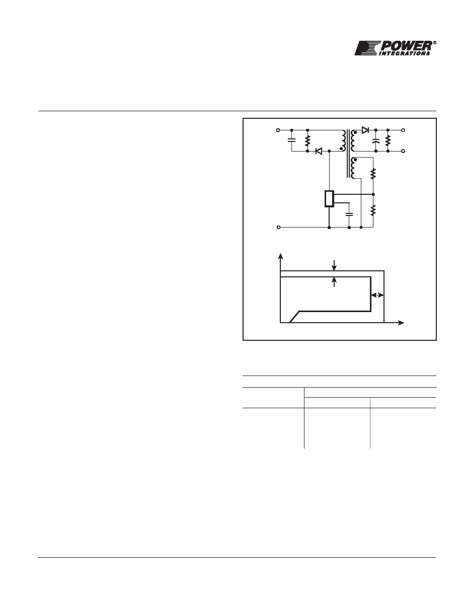
Figure 1.
Typical Application/Performance – Not a Simplied Circuit (a) and
Output Characteristic Envelope (b). (see Application Section for
more information).
LinkSwitch-II
Wide Range
HV DC Input
PI-4960-060608
D
S
FB
BP/M
I
O
V
O
±5%
±10%
PI-4906-041008
(a) Typical Application Schematic
(b) Output Characteristic
相关PDF资料 |
PDF描述 |
|---|---|
| LTC3410BESC6 | 0.63 A SWITCHING REGULATOR, 2700 kHz SWITCHING FREQ-MAX, PDSO6 |
| LM4040B30IDBZRG4 | 1-OUTPUT TWO TERM VOLTAGE REFERENCE, 3 V, PDSO3 |
| LM4040C10IDBZTG4 | 1-OUTPUT TWO TERM VOLTAGE REFERENCE, 10 V, PDSO3 |
| LQS100A48-1V5RANJ | 1-OUTPUT 200 W DC-DC REG PWR SUPPLY MODULE |
| LFD28S | 1-OUTPUT 75 W DC-DC REG PWR SUPPLY MODULE |
相关代理商/技术参数 |
参数描述 |
|---|---|
| LNK603PG | 功能描述:交流/直流开关转换器 85-265 VAC 2.5W LinkSwitch II RoHS:否 制造商:STMicroelectronics 输出电压:800 V 输入/电源电压(最大值):23.5 V 输入/电源电压(最小值):11.5 V 开关频率:115 kHz 电源电流:1.6 mA 工作温度范围:- 40 C to + 150 C 安装风格:SMD/SMT 封装 / 箱体:SSO-10 封装:Reel |
| LNK603PG-TL | 制造商:POWERINT 制造商全称:Power Integrations, Inc. 功能描述:Energy-Efficient, Accurate CV/CC Switcher for Adapters and Chargers |
| LNK604 | 制造商:POWERINT 制造商全称:Power Integrations, Inc. 功能描述:Energy-Efficient, Accurate CV/CC Switcher for Adapters and Chargers |
| LNK604DG | 功能描述:交流/直流开关转换器 3.5 W (85-265 VAC) RoHS:否 制造商:STMicroelectronics 输出电压:800 V 输入/电源电压(最大值):23.5 V 输入/电源电压(最小值):11.5 V 开关频率:115 kHz 电源电流:1.6 mA 工作温度范围:- 40 C to + 150 C 安装风格:SMD/SMT 封装 / 箱体:SSO-10 封装:Reel |
| LNK604DG-TL | 功能描述:交流/直流开关转换器 85-265 VAC 3.5W LinkSwitch II RoHS:否 制造商:STMicroelectronics 输出电压:800 V 输入/电源电压(最大值):23.5 V 输入/电源电压(最小值):11.5 V 开关频率:115 kHz 电源电流:1.6 mA 工作温度范围:- 40 C to + 150 C 安装风格:SMD/SMT 封装 / 箱体:SSO-10 封装:Reel |
发布紧急采购,3分钟左右您将得到回复。