- 您现在的位置:买卖IC网 > PDF目录22119 > LNK616PG (Power Integrations)IC OFFLINE SWIT OTP CV/CC 8DIP PDF资料下载
参数资料
| 型号: | LNK616PG |
| 厂商: | Power Integrations |
| 文件页数: | 5/18页 |
| 文件大小: | 0K |
| 描述: | IC OFFLINE SWIT OTP CV/CC 8DIP |
| 应用说明: | LinkSwitch-II Family, Appl Note AN-44 |
| 产品培训模块: | LinkSwitch-II Overview |
| 特色产品: | LinkSwitch?-II Product Family |
| 标准包装: | 50 |
| 输出隔离: | 隔离 |
| 频率范围: | 58kHz ~ 72kHz |
| 输出电压: | 700V |
| 功率(瓦特): | 6.1W |
| 工作温度: | -40°C ~ 150°C |
| 封装/外壳: | 8-DIP(0.300",7.62mm),7 引线 |
| 供应商设备封装: | DIP-8C |
| 包装: | 管件 |
| 产品目录页面: | 1202 (CN2011-ZH PDF) |
| 配用: | 596-1235-ND - KIT REF DESIGN LINKSWITCH 2 |
| 其它名称: | 596-1233-5 |
�� �
�
�LNK603-606/613-616�
�Device�
�istic� and� frequency� control� for� constant� current� (CC)� regulation.�
�The� feedback� resistors� (R5� and� R6)� were� selected� using�
�standard� 1%� resistor� values� to� center� both� the� nominal� output�
�voltage� and� constant� current� regulation� thresholds.�
�Key� Application� Considerations�
�LinkSwitch-II� Output� Cable� Voltage� Drop� Compensation�
�BYPASS� Pin� Output� Voltage�
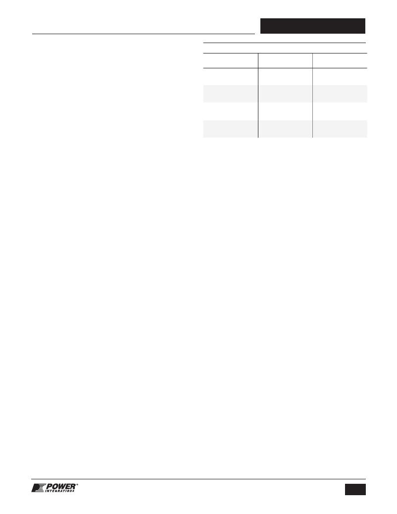
�Capacitor� Value� Change� Factor�
�1� m� F� 1.035�
�LNK613�
�10� m� F� 1.055�
�Output� Power� Table�
�LNK614�
�1� m� F�
�10� m� F�
�1.045�
�1.065�
�The� data� sheet� maximum� output� power� table� (Table� 1)� repre-�
�sents� the� maximum� practical� continuous� output� power� level�
�that� can� be� obtained� under� the� following� assumed� conditions:�
�1.� The� minimum� DC� input� voltage� is� 90� V� or� higher� at� 85� VAC�
�input.� The� value� of� the� input� capacitance� should� be� large�
�enough� to� meet� these� criteria� for� AC� input� designs.�
�2.� Secondary� output� of� 5� V� with� a� Schottky� rectifier� diode.�
�3.� Assumed� efficiency� of� 70%.�
�4.� Discontinuous� mode� operation� (K� P� >1.3).�
�5.� The� part� is� board� mounted� with� SOURCE� pins� soldered� to� a�
�sufficient� area� of� copper� to� keep� the� SOURCE� pin� tempera-�
�ture� at� or� below� 90� °C.�
�6.� Ambient� temperature� of� 50� °C� for� open� frame� designs� and�
�an� internal� enclosure� temperature� of� 60� °C� for� adapter�
�designs.�
�Note:� Higher� output� power� are� achievable� if� an� output� CC�
�tolerance� >±10%� is� acceptable,� allowing� the� device� to� be�
�operated� at� a� higher� SOURCE� pin� temperature.�
�Output� Tolerance�
�LinkSwitch-II� provides� an� overall� output� tolerance� (including� line,�
�component� variation� and� temperature)� of� ±5%� for� the� output�
�voltage� in� CV� operation� and� ±10%� for� the� output� current� during�
�CC� operation� over� a� junction� temperature� range� of� 0� °C� to� 100� °C�
�for� the� P/G� package.� For� the� D� package� (SO8)� additional� CC�
�variance� may� occur� due� to� stress� caused� by� the� manufacturing�
�flow� (i.e.� solder-wave� immersion� or� IR� reflow).� A� sample� power�
�supply� build� is� recommended� to� verify� production� tolerances� for�
�each� design.�
�BYPASS� Pin� Capacitor� Selection�
�For� LinkSwitch-II� 60x� Family� of� Devices� (without� output�
�cable� voltage� drop� compensation)�
�A� 1� m� F� BYPASS� pin� capacitor� is� recommended.� The� capacitor�
�voltage� rating� should� be� greater� than� 7� V.� The� capacitor’s�
�dielectric� material� is� not� important� but� tolerance� of� capacitor�
�should� be� ≤� ±50%.� The� capacitor� must� be� physically� located�
�close� to� the� LinkSwitch-II� BYPASS� pin.�
�For� LinkSwitch-II� 61x� Family� of� Devices� (with� output� cable�
�voltage� drop� compensation)�
�The� amount� of� output� cable� compensation� can� be� selected� with�
�the� value� of� the� BYPASS� pin� capacitor.� A� value� of� 1� m� F� selects�
�the� standard� cable� compensation.� A� 10� m� F� capacitor� selects�
�the� enhanced� cable� compensation.� Table� 2� shows� the� amount�
�of� compensation� for� each� LinkSwitch-II� device� and� capacitor�
�value.� The� capacitor� can� be� either� ceramic� or� electrolytic� but�
�tolerance� and� temperature� variation� should� be� ≤� ±50%.�
�www.powerint.com�
�1� m� F� 1.050�
�LNK615�
�10� m� F� 1.070�
�1� m� F� 1.060�
�LNK616�
�10� m� F� 1.090�
�Table� 2.� Cable� Compensation� Change� Factor� vs� Device� and� BYPASS� Pin�
�Capacitor� Value.�
�The� output� voltage� that� is� entered� into� PIXls� design� spreadsheet�
�is� the� voltage� at� the� end� of� the� output� cable� when� the� power�
�supply� is� delivering� maximum� power.� The� output� voltage� at� the�
�terminals� of� the� supply� is� the� value� measured� at� the� end� of� the�
�cable� multiplied� by� the� output� voltage� change� factor.�
�LinkSwitch-II� Layout� Considerations�
�Circuit� Board� Layout�
�LinkSwitch-II� is� a� highly� integrated� power� supply� solution� that�
�integrates� on� a� single� die,� both,� the� controller� and� the� high�
�voltage� MOSFET.� The� presence� of� high� switching� currents� and�
�voltages� together� with� analog� signals� makes� it� especially�
�important� to� follow� good� PCB� design� practice� to� ensure� stable�
�and� trouble� free� operation� of� the� power� supply.� See� Figure� 5� for�
�a� recommended� circuit� board� layout� for� LinkSwitch-II.�
�When� designing� a� printed� circuit� board� for� the� LinkSwitch-II�
�based� power� supply,� it� is� important� to� follow� the� following�
�guidelines:�
�Single� Point� Grounding�
�Use� a� single� point� (Kelvin)� connection� at� the� negative� terminal� of�
�the� input� filter� capacitor� for� the� LinkSwitch-II� SOURCE� pin� and�
�bias� winding� return.� This� improves� surge� capabilities� by�
�returning� surge� currents� from� the� bias� winding� directly� to� the�
�input� filter� capacitor.�
�Bypass� Capacitor�
�The� BYPASS� pin� capacitor� should� be� located� as� close� as�
�possible� to� the� SOURCE� and� BYPASS� pins.�
�Feedback� Resistors�
�Place� the� feedback� resistors� directly� at� the� FEEDBACK� pin� of�
�the� LinkSwitch-II� device.� This� minimizes� noise� coupling.�
�Thermal� Considerations�
�The� copper� area� connected� to� the� SOURCE� pins� provides� the�
�LinkSwitch-II� heat� sink.� A� good� estimate� is� that� the� LinkSwitch-II�
�will� dissipate� 10%� of� the� output� power.� Provide� enough� copper�
�area� to� keep� the� SOURCE� pin� temperature� below� 90� °C.� Higher�
�temperatures� are� allowable� only� if� an� output� current� (CC)�
�tolerance� above� ±10%� is� acceptable.� In� this� case� a� maximum�
�SOURCE� pin� temperature� below� 110� °C� is� recommended� to�
�provide� margin� for� part� to� part� R� DS(ON)� variation.�
�5�
�Rev.� F� 01/10�
�相关PDF资料 |
PDF描述 |
|---|---|
| ACM28DRST-S288 | CONN EDGECARD EXTEND 56POS 0.156 |
| VE-BWD-CY-F1 | CONVERTER MOD DC/DC 85V 50W |
| TPME687K006R0023 | CAP TANT 680UF 6.3V 10% 2917 |
| LC4032V-5T44I | IC PLD 32MC 30I/O 5NS 44TQFP |
| AYM22DTBN-S189 | CONN EDGECARD 44POS R/A .156 SLD |
相关代理商/技术参数 |
参数描述 |
|---|---|
| LNK616PG-TL | 制造商:POWERINT 制造商全称:Power Integrations, Inc. 功能描述:Energy-Efficient, Accurate CV/CC Switcher for Adapters and Chargers |
| LNK623 | 制造商:POWERINT 制造商全称:Power Integrations, Inc. 功能描述:Energy-Effi cient, Off-line Switcher with Accurate Primary-side Constant-Voltage (CV) Control |
| LNK623DG | 功能描述:交流/直流开关转换器 5.0 W (85-265 VAC) RoHS:否 制造商:STMicroelectronics 输出电压:800 V 输入/电源电压(最大值):23.5 V 输入/电源电压(最小值):11.5 V 开关频率:115 kHz 电源电流:1.6 mA 工作温度范围:- 40 C to + 150 C 安装风格:SMD/SMT 封装 / 箱体:SSO-10 封装:Reel |
| LNK623DG-TL | 功能描述:交流/直流开关转换器 5.0 W (85-265 VAC) RoHS:否 制造商:STMicroelectronics 输出电压:800 V 输入/电源电压(最大值):23.5 V 输入/电源电压(最小值):11.5 V 开关频率:115 kHz 电源电流:1.6 mA 工作温度范围:- 40 C to + 150 C 安装风格:SMD/SMT 封装 / 箱体:SSO-10 封装:Reel |
| LNK623PG | 功能描述:交流/直流开关转换器 5.0 W (85-265 VAC) RoHS:否 制造商:STMicroelectronics 输出电压:800 V 输入/电源电压(最大值):23.5 V 输入/电源电压(最小值):11.5 V 开关频率:115 kHz 电源电流:1.6 mA 工作温度范围:- 40 C to + 150 C 安装风格:SMD/SMT 封装 / 箱体:SSO-10 封装:Reel |
发布紧急采购,3分钟左右您将得到回复。