- 您现在的位置:买卖IC网 > PDF目录79707 > LOG114AIRGVR (TEXAS INSTRUMENTS INC) LOG OR ANTILOG AMPLIFIER, PQCC16 PDF资料下载
参数资料
| 型号: | LOG114AIRGVR |
| 厂商: | TEXAS INSTRUMENTS INC |
| 元件分类: | 模拟运算功能 |
| 英文描述: | LOG OR ANTILOG AMPLIFIER, PQCC16 |
| 封装: | 4 X 4 MM, GREEN, PLASTIC, QFN-16 |
| 文件页数: | 7/29页 |
| 文件大小: | 637K |
| 代理商: | LOG114AIRGVR |
第1页第2页第3页第4页第5页第6页当前第7页第8页第9页第10页第11页第12页第13页第14页第15页第16页第17页第18页第19页第20页第21页第22页第23页第24页第25页第26页第27页第28页第29页
LOG114
SBOS301A MAY 2004 REVISED MARCH 2007
www.ti.com
15
A4
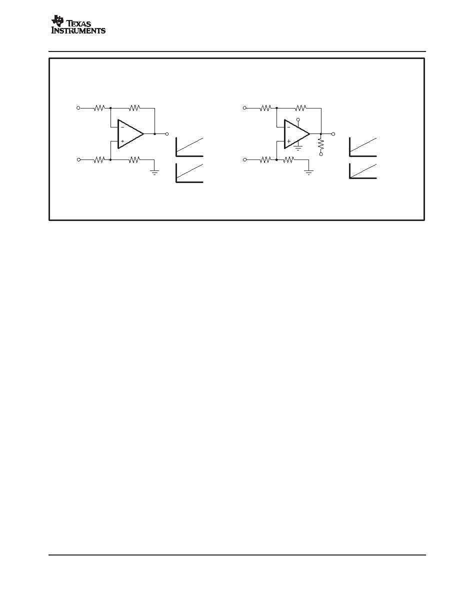
OPA335
Internal A4 Output Amplifier
External Output Amplifier
+5V
R
5
100k
V
REF
+2.5V
V
LOGOUT
V
LOGOUT
VO4 = 2/3 (VLOGOUT) + 3.16
I2
100pA
10mA
VOUT = 2.5/3 (VLOGOUT)+ 3.3
a) A4 amplifier used to scale and offset VLOGOUT for 0.5V to 2.5V output.
b) OPA335 amplifier used to scale and offset VLOGOUT for 0V to 2.5V output.
NOTE: (1) See OPA335 data sheet for use of R
P connected to 5V to achieve 0V output.
R
6
66.5k
R7
100k
R8
316k
R
5
100k
V
REF
+2.5V
R
6
82.5k
RP(1)
5V
R7
100k
R8
267k
V
O4
0.5V
2.5V
I2
100pA
10mA
V
OUT
0.5V
2.5V
Figure 4. Operational Amplifier Configuration for Scaling and Offsetting the Output Going to ADC Stage.
ADVANTAGES OF DUALSUPPLY OPERATION
The LOG114 performs very well on a single +5V supply
by level-shifting pin 7 (Com) to half-supply and raising
the common-mode voltage (pin 5, VCM IN) of the input
amplifiers. This levelshift places the input amplifiers in
the linear operating range. However, there are also
some advantages to operating the LOG114 on dual
±5V
supplies. These advantages include:
1) eliminating the need for the +4.096V precision
reference;
2) eliminating a small additional source of error arising
from the noise and temperature drift of the levelshifting
voltage; and
3) allowing increased magnitude of a reverse bias
voltage on the photodiode.
COM (PIN 7) VOLTAGE RANGE
The voltage on the Com pin is used to bias the differen-
tial amplifier, A3, within its linear range. This voltage can
provide an asymmetrical offset of the VLOGOUT voltage.
VCM IN (Pin 5)
The VCMIN pin is used to bias the A1 and A2 amplifier into
its common-mode input voltage range, (V) + 1.5V to
(V+) 1.5V.
INPUT CURRENT RANGE
To maintain specified accuracy, the input current range
of the LOG114 should be limited from 100pA to 3.5mA.
Input currents outside of this range may compromise
the LOG114 performance. Input currents larger than
3.5mA result in increased nonlinearity. An absolute
maximum input current rating of 10mA is included to
prevent excessive power dissipation that may damage
the input transistor.
相关PDF资料 |
PDF描述 |
|---|---|
| LTC4075XEDD#TR | 1-CHANNEL POWER SUPPLY SUPPORT CKT, PDSO10 |
| LTC3835EUFD#PBF | 3 A SWITCHING CONTROLLER, 580 kHz SWITCHING FREQ-MAX, PQCC20 |
| LM4040CYM3-2.5TR | 1-OUTPUT TWO TERM VOLTAGE REFERENCE, 2.5 V, PDSO3 |
| LES10A48-5V0REJ | 1-OUTPUT 50 W DC-DC REG PWR SUPPLY MODULE |
| LT3467AIDDB#TRPBF | 2.5 A SWITCHING REGULATOR, 2700 kHz SWITCHING FREQ-MAX, PDSO8 |
相关代理商/技术参数 |
参数描述 |
|---|---|
| LOG114AIRGVRG4 | 功能描述:对数放大器 Prec High-Speed Logarithmic Amp RoHS:否 制造商:Texas Instruments 通道数量:3 带宽:3 dB 共模抑制比(最小值): 输入补偿电压:+/- 7 mV 输入电压范围(最大值):5.5 V 工作电源电压:4.5 V to 5.5 V 电源电流:+/- 15 mA 工作温度范围:- 40 C to +85 C 安装风格:SMD/SMT 封装 / 箱体:VQFN-16 封装:Reel |
| LOG114AIRGVT | 功能描述:对数放大器 Precision High-Speed RoHS:否 制造商:Texas Instruments 通道数量:3 带宽:3 dB 共模抑制比(最小值): 输入补偿电压:+/- 7 mV 输入电压范围(最大值):5.5 V 工作电源电压:4.5 V to 5.5 V 电源电流:+/- 15 mA 工作温度范围:- 40 C to +85 C 安装风格:SMD/SMT 封装 / 箱体:VQFN-16 封装:Reel |
| LOG114AIRGVTG4 | 功能描述:对数放大器 Prec High-Speed Logarithmic Amp RoHS:否 制造商:Texas Instruments 通道数量:3 带宽:3 dB 共模抑制比(最小值): 输入补偿电压:+/- 7 mV 输入电压范围(最大值):5.5 V 工作电源电压:4.5 V to 5.5 V 电源电流:+/- 15 mA 工作温度范围:- 40 C to +85 C 安装风格:SMD/SMT 封装 / 箱体:VQFN-16 封装:Reel |
| LOG114EVM | 功能描述:放大器 IC 开发工具 LOG114 Eval Mod RoHS:否 制造商:International Rectifier 产品:Demonstration Boards 类型:Power Amplifiers 工具用于评估:IR4302 工作电源电压:13 V to 23 V |
| LOG1527 | 制造商:未知厂家 制造商全称:未知厂家 功能描述:由CMOS工艺设计制造的可内烧的学习码编码IC. |
发布紧急采购,3分钟左右您将得到回复。