- 您现在的位置:买卖IC网 > PDF目录80262 > LOG2112AIDWR (TEXAS INSTRUMENTS INC) LOG OR ANTILOG AMPLIFIER, 1.4 MHz BAND WIDTH, PDSO16 PDF资料下载
参数资料
| 型号: | LOG2112AIDWR |
| 厂商: | TEXAS INSTRUMENTS INC |
| 元件分类: | 模拟运算功能 |
| 英文描述: | LOG OR ANTILOG AMPLIFIER, 1.4 MHz BAND WIDTH, PDSO16 |
| 封装: | ROHS COMPLIANT, PLASTIC, MS-013AA, SOIC-16 |
| 文件页数: | 18/20页 |
| 文件大小: | 621K |
| 代理商: | LOG2112AIDWR |
LOG112, 2112
7
SBOS246D
www.ti.com
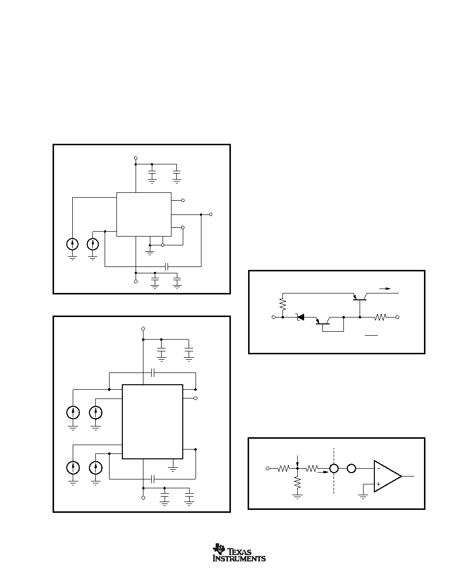
FIGURE 1. Basic Connections of the LOG112.
APPLICATION INFORMATION
The LOG112 is a true logarithmic amplifier that uses the
base-emitter voltage relationship of bipolar transistors to
compute the logarithm, or logarithmic ratio of a current ratio.
Figure 1 and Figure 2 show the basic connections required
for operation of the LOG112 and LOG2112. In order to
reduce the influence of lead inductance of power-supply
lines, it is recommended that each supply be bypassed with
a 10
F tantalum capacitor in parallel with a 1000pF ceramic
capacitor, as shown in Figure 1 and Figure 2. Connecting
the capacitors as close to the LOG112 and LOG2112 as
possible will contribute to noise reduction as well.
INPUT CURRENT RANGE
To maintain specified accuracy, the input current range of the
LOG112 and LOG2112 should be limited from 100pA to
3.5mA. Input currents outside of this range may compromise
the LOG112 performance. Input currents larger than 3.5mA
result in increased nonlinearity. An absolute maximum input
current rating of 10mA is included to prevent excessive power
dissipation that may damage the input transistor.
On
±5V supplies, the total input current (I
1 + I2) is limited to
4.5mA. Due to compliance issues internal to the LOG112 and
LOG2112, to accommodate larger total input currents, supplies
should be increased.
SETTING THE REFERENCE CURRENT
When the LOG112 and LOG2112 are used to compute loga-
rithms, either I1 or I2 can be held constant to become the
reference current to which the other is compared.
VLOGOUT is expressed as:
VLOGOUT = (0.5V)LOG (I1/IREF)
(1)
IREF can be derived from an external current source (such as
that shown in Figure 3), or it may be derived from a voltage
source with one or more resistors. When a single resistor is
used, the value may be large depending on IREF. If IREF is
10nA and +2.5V is used:
RREF = 2.5V/10nA = 250M
(2)
14
1
5
8
6
910
13
V–
V+
10
F
LOG112
1000pF
10
F
1000pF
I
1
I
2
V
LOGOUT
V
REF
11
V
REF – GND
V
CM – IN
C
15
16
5
6
11
8
V–
V+
10
F
LOG2112
1000pF
10
F
1000pF
I
1B
I
2B
1
2
I
2A
I
1A
V
LOGOUTA
9
V
REF
12
V
LOGOUTB
C
CB
C
CA
FIGURE 2. Basic Connections of the LOG2112.
FIGURE 3. Temperature Compensated Current Source.
2N2905
I
REF
R
REF
2N2905
+15V
–15V
I
REF =
6V
R
REF
3.6k
6V
IN834
FIGURE 4. T Network for Reference Current.
A
1
+
R
2
R
1
+5V
R
3
V
REF = 100mV
R
3 >> R2
I
REF
–
V
OS
1
A voltage divider may be used to reduce the value of the
resistor, as shown in Figure 4. When using this method, one
must consider the possible errors caused by the amplifier’s
input offset voltage. The input offset voltage of amplifier A1
has a maximum value of 1.5mV, making VREF a suggested
value of 100mV.
相关PDF资料 |
PDF描述 |
|---|---|
| LW005F | DC-DC REG PWR SUPPLY MODULE |
| LCD15-24S12W-A | 1-OUTPUT 15 W DC-DC REG PWR SUPPLY MODULE |
| LCD15-48D12W-A | 2-OUTPUT 15 W DC-DC REG PWR SUPPLY MODULE |
| LK2540-7ERD3TB1 | 2-OUTPUT 150 W AC-DC REG PWR SUPPLY MODULE |
| LK2540-7ERD5TB1 | 2-OUTPUT 150 W AC-DC REG PWR SUPPLY MODULE |
相关代理商/技术参数 |
参数描述 |
|---|---|
| LOG2112AIDWRE4 | 功能描述:对数放大器 Precision Log & Log Ratio Amp RoHS:否 制造商:Texas Instruments 通道数量:3 带宽:3 dB 共模抑制比(最小值): 输入补偿电压:+/- 7 mV 输入电压范围(最大值):5.5 V 工作电源电压:4.5 V to 5.5 V 电源电流:+/- 15 mA 工作温度范围:- 40 C to +85 C 安装风格:SMD/SMT 封装 / 箱体:VQFN-16 封装:Reel |
| LOGIC | 制造商:SALEAE LLC 功能描述:8 Channel Logic Analyzer |
| LOGIC PCBA | 制造商:Misc 功能描述: |
| LOGIC SIZE 11 | 制造商:DEWALT 功能描述:DEWALT LOGIC SIZE 11 |
| LOGIC SIZE 9 | 制造商:DEWALT 功能描述:DEWALT LOGIC SIZE 9 |
发布紧急采购,3分钟左右您将得到回复。