- 您现在的位置:买卖IC网 > PDF目录19381 > LP2950CDT-5.0 (ON Semiconductor)IC REG LDO 5V .1A DPAK PDF资料下载
参数资料
| 型号: | LP2950CDT-5.0 |
| 厂商: | ON Semiconductor |
| 文件页数: | 6/22页 |
| 文件大小: | 0K |
| 描述: | IC REG LDO 5V .1A DPAK |
| 产品变化通告: | LTB Notification 03/Jan/2008 |
| 标准包装: | 75 |
| 稳压器拓扑结构: | 正,固定式 |
| 输出电压: | 5V |
| 输入电压: | 最高 30V |
| 电压 - 压降(标准): | 0.35V @ 100mA |
| 稳压器数量: | 1 |
| 电流 - 输出: | 100mA |
| 工作温度: | -40°C ~ 125°C |
| 安装类型: | 表面贴装 |
| 封装/外壳: | TO-252-3,DPak(2 引线+接片),SC-63 |
| 供应商设备封装: | DPAK-3 |
| 包装: | 管件 |
| 其它名称: | LP2950CDT-5.0OS |
�� �
�
�LP2950,� LP2951,� NCV2951�
�DEFINITIONS�
�Dropout� Voltage� ?� The� input/output� voltage� differential�
�at� which� the� regulator� output� no� longer� maintains� regulation�
�against� further� reductions� in� input� voltage.� Measured� when�
�the� output� drops� 100� mV� below� its� nominal� value� (which� is�
�measured� at� 1.0� V� differential),� dropout� voltage� is� affected�
�by� junction� temperature,� load� current� and� minimum� input�
�supply� requirements.�
�Line� Regulation� ?� The� change� in� output� voltage� for� a�
�change� in� input� voltage.� The� measurement� is� made� under�
�conditions� of� low� dissipation� or� by� using� pulse� techniques�
�such� that� average� chip� temperature� is� not� significantly�
�affected.�
�Load� Regulation� ?� The� change� in� output� voltage� for� a�
�change� in� load� current� at� constant� chip� temperature.�
�Maximum� Power� Dissipation� ?� The� maximum� total�
�device� dissipation� for� which� the� regulator� will� operate�
�within� specifications.�
�Bias� Current� ?� Current� which� is� used� to� operate� the�
�regulator� chip� and� is� not� delivered� to� the� load.�
�10�
�Output� Noise� Voltage� ?� The� RMS� ac� voltage� at� the�
�output,� with� constant� load� and� no� input� ripple,� measured�
�over� a� specified� frequency� range.�
�Leakage� Current� ?� Current� drawn� through� a� bipolar�
�transistor� collector� ?� base� junction,� under� a� specified�
�collector� voltage,� when� the� transistor� is� “off”.�
�Upper� Threshold� Voltage� ?� Voltage� applied� to� the�
�comparator� input� terminal,� below� the� reference� voltage�
�which� is� applied� to� the� other� comparator� input� terminal,�
�which� causes� the� comparator� output� to� change� state� from� a�
�logic� “0”� to� “1”.�
�Lower� Threshold� Voltage� ?� Voltage� applied� to� the�
�comparator� input� terminal,� below� the� reference� voltage�
�which� is� applied� to� the� other� comparator� input� terminal,�
�which� causes� the� comparator� output� to� change� state� from� a�
�logic� “1”� to� “0”.�
�Hysteresis� ?� The� difference� between� Lower� Threshold�
�voltage� and� Upper� Threshold� voltage.�
�6.0�
�LP2951C�
�5.0�
�T� A� =� 25� ?� C�
�1.0�
�0.1�
�4.0�
�3.0�
�2.0�
�1.0�
�R� L� = 50 k� W�
�R� L� =� 50� W�
�0.01�
�0.1�
�1.0�
�10�
�100�
�0�
�0�
�1.0�
�2.0�
�3.0�
�4.0�
�5.0�
�6.0�
�5.00�
�4.99�
�I� L� ,� LOAD� CURRENT� (mA)�
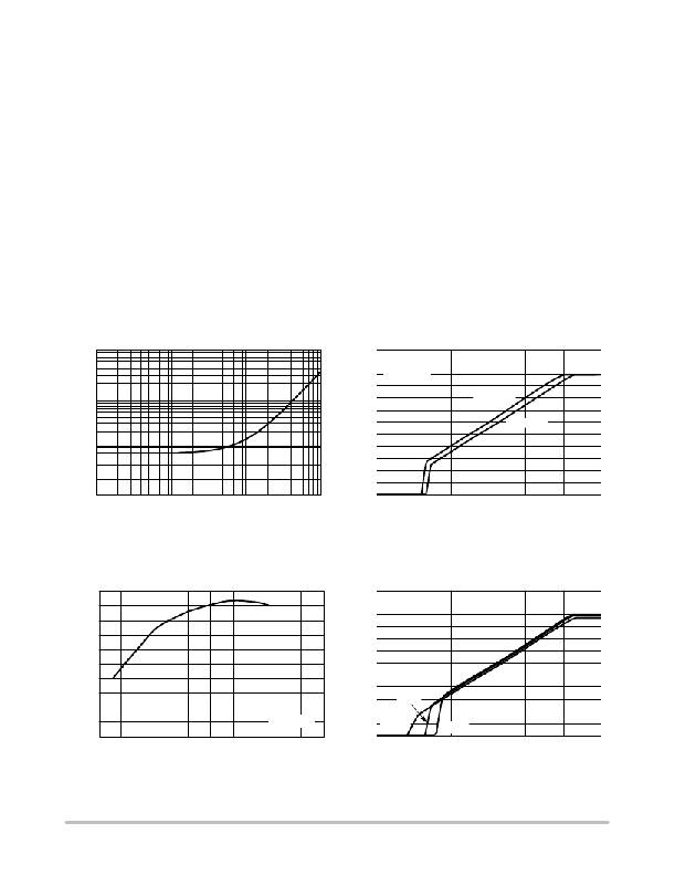
�Figure� 2.� Quiescent� Current�
�6.0�
�5.0�
�V� in� ,� INPUT� VOLTAGE� (V)�
�Figure� 3.� 5.0� V� Dropout� Characteristics� over�
�Load�
�LP2951C�
�4.0�
�4.98�
�3.0�
�4.97�
�2.0�
�4.96�
�1.0�
�25� ?� C�
�4.95�
�-� 50�
�0�
�50�
�100�
�LP2951C�
�150�
�200�
�0�
�0�
�125� ?� C�
�1.0�
�?� 40� ?� C�
�2.0�
�3.0�
�4.0�
�5.0�
�6.0�
�T� A� ,� AMBIENT� TEMPERATURE� (� ?� C)�
�Figure� 4.� Output� Voltage� versus� Temperature�
�V� in� ,� INPUT� VOLTAGE� (V)�
�Figure� 5.� 5.0� V� Dropout� Characteristics� with�
�R� L� =� 50� W�
�http://onsemi.com�
�6�
�相关PDF资料 |
PDF描述 |
|---|---|
| TPSC226K016R0150 | CAP TANT 22UF 16V 10% 2312 |
| ADSP-21161NYCAZ110 | IC DSP CONTROLLER 32BIT 225BGA |
| EB63-S0C0640W | CONN EDGEBOARD DUAL 12POS 3A |
| VI-B2R-CY-F3 | CONVERTER MOD DC/DC 7.5V 50W |
| 1-1734344-1 | CONN D-SUB 15POS RCPT R/A DIP |
相关代理商/技术参数 |
参数描述 |
|---|---|
| LP2950CDTX-3.0 | 功能描述:低压差稳压器 - LDO RoHS:否 制造商:Texas Instruments 最大输入电压:36 V 输出电压:1.4 V to 20.5 V 回动电压(最大值):307 mV 输出电流:1 A 负载调节:0.3 % 输出端数量: 输出类型:Fixed 最大工作温度:+ 125 C 安装风格:SMD/SMT 封装 / 箱体:VQFN-20 |
| LP2950CDTX-3.0/NOPB | 功能描述:低压差稳压器 - LDO RoHS:否 制造商:Texas Instruments 最大输入电压:36 V 输出电压:1.4 V to 20.5 V 回动电压(最大值):307 mV 输出电流:1 A 负载调节:0.3 % 输出端数量: 输出类型:Fixed 最大工作温度:+ 125 C 安装风格:SMD/SMT 封装 / 箱体:VQFN-20 |
| LP2950CDTX-3.3 | 功能描述:低压差稳压器 - LDO RoHS:否 制造商:Texas Instruments 最大输入电压:36 V 输出电压:1.4 V to 20.5 V 回动电压(最大值):307 mV 输出电流:1 A 负载调节:0.3 % 输出端数量: 输出类型:Fixed 最大工作温度:+ 125 C 安装风格:SMD/SMT 封装 / 箱体:VQFN-20 |
| LP2950CDTX-3.3/NOPB | 功能描述:低压差稳压器 - LDO RoHS:否 制造商:Texas Instruments 最大输入电压:36 V 输出电压:1.4 V to 20.5 V 回动电压(最大值):307 mV 输出电流:1 A 负载调节:0.3 % 输出端数量: 输出类型:Fixed 最大工作温度:+ 125 C 安装风格:SMD/SMT 封装 / 箱体:VQFN-20 |
| LP2950CDTX-5.0 | 功能描述:低压差稳压器 - LDO RoHS:否 制造商:Texas Instruments 最大输入电压:36 V 输出电压:1.4 V to 20.5 V 回动电压(最大值):307 mV 输出电流:1 A 负载调节:0.3 % 输出端数量: 输出类型:Fixed 最大工作温度:+ 125 C 安装风格:SMD/SMT 封装 / 箱体:VQFN-20 |
发布紧急采购,3分钟左右您将得到回复。