- 您现在的位置:买卖IC网 > PDF目录53664 > LQN-2/50-D12B (CD TECHNOLOGIES INC) 1-OUTPUT DC-DC REG PWR SUPPLY MODULE PDF资料下载
参数资料
| 型号: | LQN-2/50-D12B |
| 厂商: | CD TECHNOLOGIES INC |
| 元件分类: | 电源模块 |
| 英文描述: | 1-OUTPUT DC-DC REG PWR SUPPLY MODULE |
| 文件页数: | 2/9页 |
| 文件大小: | 609K |
| 代理商: | LQN-2/50-D12B |
LXN D12 Series
N O N - I S O L A T E D , 4 5 - 5 0 A Q U A R T E R B R I C K , D C / D C C O N V E R T E R S
2
LQN-0.8/50-D12
0.8
50
30
50
±0.25%
12
10.2-13.8
TBD
TBD%
83%
C41,C42, P62
LQN-1/50-D12
1
50
30
50
±0.25%
12
10.2-13.8
TBD
TBD%
85%
86%
C41,C42, P62
LQN-1.2/50-D12
1.2
50
30
50
±0.25%
12
10.2-13.8
TBD
TBD%
87%
87.5%
C41,C42, P62
LQN-1.5/50-D12
1.5
50
20
50
±0.25%
12
10.2-13.8
TBD
TBD%
88%
C41,C42, P62
LQN-1.8/50-D12
1.8
50
20
50
±0.25%
12
10.2-13.8
TBD
TBD%
89.5%
C41,C42, P62
LQN-2/50-D12
2
50
20
50
±0.25%
12
10.2-13.8
TBD
TBD%
90%
C41,C42, P62
LQN-2.5/45-D12
2.5
45
20
50
±0.25%
12
10.2-13.8
TBD
TBD%
91.5%
92%
C41,C42, P62
LQN-3.3/45-D12
3.3
45
30
50
±0.25%
12
10.2-13.8
TBD
TBD%
93%
93.5%
C41,C42, P62
LQN-5/45-D12
5
45
30
50
±0.25%
12
10.2-13.8
TBD
TBD%
95%
95.5%
C41,C42, P62
Typical at TA = +25°C under nominal line voltage and full-load conditions, unless otherwise
noted. All models are tested and specied with external 33F input capacitor and 470F
poscap output capacitor paralleled with a 100F ceramic output capacitor.
Ripple/Noise (R/N) is tested/specied over a 20MHz bandwidth.
These devices have no minimum-load requirements and will regulate under no-load conditions.
Regulation specications describe the output-voltage deviation as the line voltage or load is
varied from its nominal/midpoint value to either extreme.
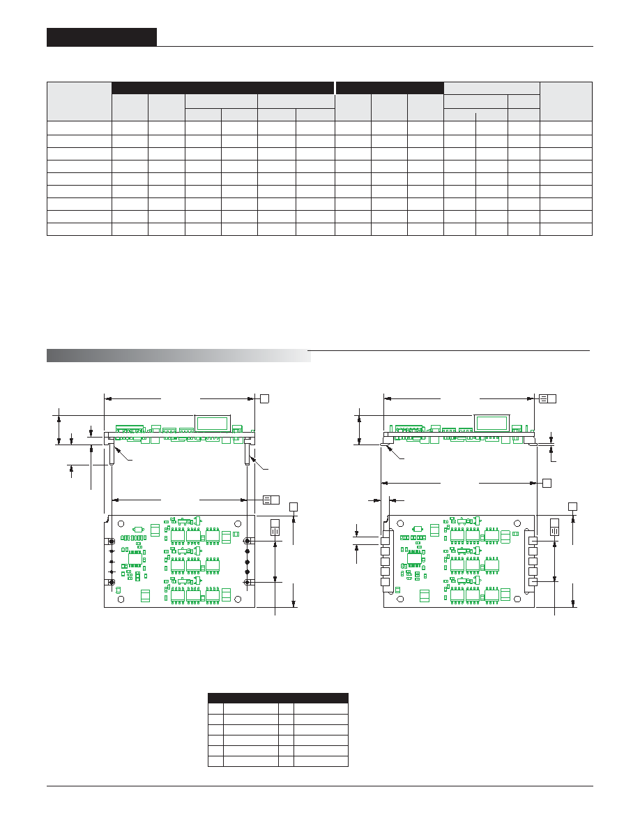
M E C H A N I C A L
S P E C I F I C A T I O N S
Nominal line voltage, no-load/full-load conditions.
The operating input voltage is 10.2V to 13.8V. However, 10.8VIN is required for the DC/DC
to properly start up under all line, load and temperature conditions. The 10.8V potential must be
maintained across the inputs until the output is up and regulating. After the output is regulating,
the operating input range is 10.2V to 13.8V.
Performance Specications and Ordering Guide
Package
VOUT
IOUT
VIN Nom. Range
IIN
(Case,
Model
(Volts)
(Amps)
Typ.
Max.
Line
Load
(Volts)
(mA/A)
Min.
Typ.
Pinout)
Output
Input
R/N (mVp-p)
Regulation (Max.)
Efciency
Full Load
Load
Pin
Function P62
Pin
Function P62
1
Input Common
6
Output Common
2
VOUT Trim
7
+Output
3
N.C.*
8
Output Common
4
On/Off Control
9
+Output
5
+Input
10
+Sense In
I/O Connections
C41 Through-Hole Package
C42 Surface-Mount Package
See page 9 for Part Number Structure.
* A "Power Good" output is available
on pin 3 under special order.
Contact DATEL.
相关PDF资料 |
PDF描述 |
|---|---|
| LQN-3.3/45-D12MH | 1-OUTPUT 150 W DC-DC REG PWR SUPPLY MODULE |
| LQN-0.8/50-D12MB | 1-OUTPUT DC-DC REG PWR SUPPLY MODULE |
| LQN-1.5/50-D12M | 1-OUTPUT DC-DC REG PWR SUPPLY MODULE |
| LQN-3.3/45-D12B | 1-OUTPUT 150 W DC-DC REG PWR SUPPLY MODULE |
| LQN-3.3/45-D12H | 1-OUTPUT 150 W DC-DC REG PWR SUPPLY MODULE |
相关代理商/技术参数 |
参数描述 |
|---|---|
| LQN2A18NM04M00 | 制造商:MUR 功能描述:LQN2A18NM04M00 |
| LQN2A47NM04M00 | 制造商:Murata Manufacturing Co Ltd 功能描述: |
| LQN2A56NM04M | 制造商:Murata Manufacturing Co Ltd 功能描述: |
| LQN2AR15K04M00 | 制造商:MUR 功能描述:IND |
| LQN2AR15K04M00-01 | 制造商:Murata Manufacturing Co Ltd 功能描述:1 ELEMENT, 0.15 uH, ALUMINA-CORE, GENERAL PURPOSE INDUCTOR, SMD |
发布紧急采购,3分钟左右您将得到回复。