参数资料
| 型号: | LT1002CN#PBF |
| 厂商: | Linear Technology |
| 文件页数: | 16/16页 |
| 文件大小: | 0K |
| 描述: | IC PREC OPAMP DUAL MATCHED 14DIP |
| 标准包装: | 25 |
| 放大器类型: | 通用 |
| 电路数: | 2 |
| 转换速率: | 0.25 V/µs |
| 增益带宽积: | 800kHz |
| 电流 - 输入偏压: | 700pA |
| 电压 - 输入偏移: | 25µV |
| 电压 - 电源,单路/双路(±): | ±3 V ~ 18 V |
| 工作温度: | 0°C ~ 70°C |
| 安装类型: | 通孔 |
| 封装/外壳: | 14-DIP(0.300",7.62mm) |
| 供应商设备封装: | 14-PDIP |
| 包装: | 管件 |
| 产品目录页面: | 1317 (CN2011-ZH PDF) |
9
LT1002
1002fb
APPLICATIONS INFORMATION
WU
U
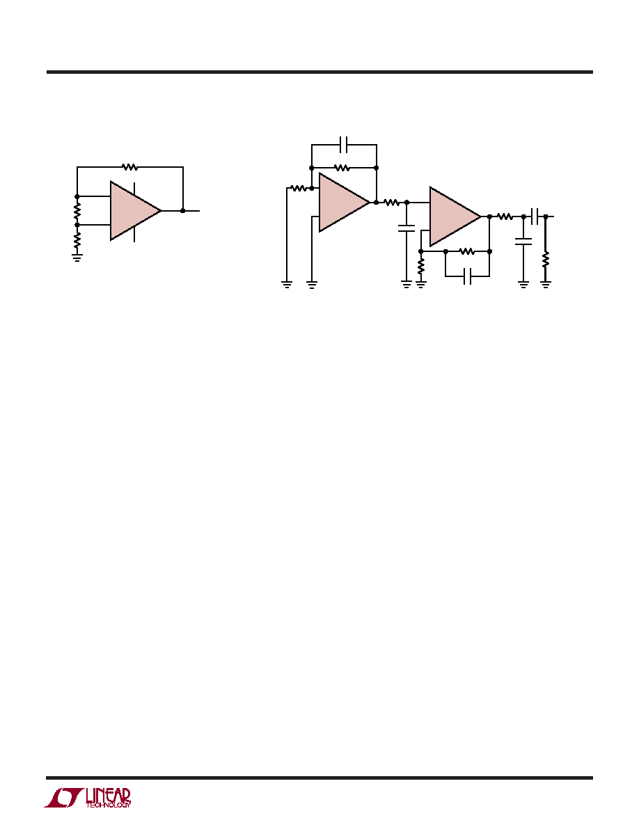
Test Circuit for Offset Voltage
and its Drift with Temperature
–
+
–15V
15V
50k*
100
*
50k*
3
(10)
(11)
4
14 (7)
13 (6)
VO
1002 TA05
VO = 1000 VOS
* RESISTORS MUST HAVE LOW
THERMOELECTRIC POTENTIAL.
12 (5)
1/2
LT1002
0.1Hz to 10Hz Noise Test Circuit
–
+
–
+
100k
2k
100k
4.3k
110k
SCOPE
× 1
RIN = 1M
0.1
F
4.7
F
24.3k
10
1002 TA06
0.1
F
22
F
VOLTAGE GAIN = 50,000
2.2
F
DEVICE
UNDER
TEST
A
1/2 LT1002
B
1/2 LT1002
PEAK TO PEAK NOISE MEASURED IN 10 SEC INTERVAL
This circuit is also used as burn-in configuration for the
LT1002, with supply voltages increased to
±20V.
Unless proper care is exercised, thermocouple effects,
caused by temperature gradients across dissimilar metals
at the contacts to the input terminals, can exceed the
inherent drift of the amplifier. Air currents should be
minimized, package leads should be short, the two input
leads should be as close together as possible and main-
tained at the same temperature.
Channel Separation
This parameter is defined as the ratio of the change in input
offset voltage of one amplifier to the change in output
voltage of the other amplifier causing the offset change.
At low frequencies the LT1002’s channel separation is an
almost unmeasurable 148dB. As frequency increases, pin
to pin capacitance of the package, between the output of
one amplifier and the inputs of the other, becomes domi-
nant. Since these pins are non-adjacent, the capacitance is
only 0.02pF. To maintain the LT1002’s excellent channel
separation at higher frequencies, the socket and PC board
capacitances should be minimized.
The device under test should be warmed up for three
minutes and shielded from air currents. Turn the device
180
° to measure the noise of side B.
Power supplies
The LT1002 is specified over a wide range of power supply
voltages from
±3V to ±18V. Operation with lower supplies
is possible, down to
±1.2V (two Ni-Cad batteries). How-
ever, with
±1.2V supplies, the device is stable only in
closed loop gains of + 2 or higher (or inverting gain of one
or higher).
The V+ supply terminals are completely independent and
may be powered by separate supplies if desired (this
approach, however, would sacrifice the advantages of the
power supply rejection ratio matching). The V– supply
terminals are both connected to the common substrate
and must be tied to the same voltage. Both V – pins should
be used.
相关PDF资料 |
PDF描述 |
|---|---|
| TSW-105-14-S-S | CONN HEADER 5POS .100" SGL GOLD |
| TSW-102-08-L-D-RA | CONN HEADER 4POS .100 DL R/A AU |
| TSW-108-07-T-D | CONN HEADER 16POS .100" DL TIN |
| TSW-113-07-L-S | CONN HEADER 13POS .100" SGL GOLD |
| 929835-01-21-RK | CONN HEADER .100 SNGL R/A 21POS |
相关代理商/技术参数 |
参数描述 |
|---|---|
| LT1002M | 制造商:LINER 制造商全称:Linear Technology 功能描述:Dual, Matched Precision Operational Amplifier |
| LT1002MJ | 制造商:Linear Technology 功能描述:OP Amp Dual GP 制造商:Linear Technology 功能描述:OP Amp Dual GP ±22V 14-Pin CDIP |
| LT1002MJ/883 | 制造商:Linear Technology 功能描述:OP Amp Dual GP ±22V 14-Pin CDIP |
| LT1003 | 制造商:LINER 制造商全称:Linear Technology 功能描述:5 Volt, 5 Amp Voltage Regulator |
| LT1003C | 制造商:LINER 制造商全称:Linear Technology 功能描述:5 Volt, 5 Amp Voltage Regulator |
发布紧急采购,3分钟左右您将得到回复。