参数资料
| 型号: | LT1006CN8#PBF |
| 厂商: | Linear Technology |
| 文件页数: | 2/16页 |
| 文件大小: | 0K |
| 描述: | IC PREC OP-AMP 5V SINGLE 8-DIP |
| 标准包装: | 50 |
| 放大器类型: | 通用 |
| 电路数: | 1 |
| 转换速率: | 1.2 V/µs |
| 电流 - 输入偏压: | 10nA |
| 电压 - 输入偏移: | 30µV |
| 电流 - 电源: | 360µA |
| 电压 - 电源,单路/双路(±): | 5 V ~ 30 V,±2.5 V ~ 15 V |
| 工作温度: | 0°C ~ 70°C |
| 安装类型: | 通孔 |
| 封装/外壳: | 8-DIP(0.300",7.62mm) |
| 供应商设备封装: | 8-PDIP |
| 包装: | 管件 |
| 产品目录页面: | 1317 (CN2011-ZH PDF) |
10
LT1006
1006fa
In automated production testing the output is forced to
1.4V by the test loop; offset voltage is measured with a
common mode voltage of zero and the negative supply at
zero (Pin 4). Without the test loop, these exact conditions
cannot be achieved. The test circuit shown ensures that
the output will never saturate even with worst-case offset
voltages (– 250V over the – 55°C to 125°C range). The
effective common mode input is 0.3V with respect to the
negative supply. As indicated by the common mode rejec-
tion specifications the difference is only a few microvolts
between the two methods of offset voltage measurement.
Low Supply Operation
The minimum guaranteed supply voltage for proper
operation of the LT1006 is 2.7V. Typical supply current at
this voltage is 320A; therefore, power dissipation is only
860W.
Noise Testing
For application information on noise testing and
calculations, please see the LT1007 or LT1028 data sheet.
Supply Current Programming
Connecting an optional external resistor to Pin 8 changes
the biasing of the LT1006 in order to increase its speed or
to decrease its power consumption. If a higher slew rate is
required, connect the external resistor for Pin 8 to Pin 4
[see performance curves for Increasing Slew Rate
(RSET to V–)]. For lower power consumption, inject a
current into Pin 8 (which is approximately 60mV above
V–) as shown on the Reducing Power Dissipation plot.
This can be accomplished by connecting RSET to the
positive supply, or to save additional power, by obtaining
the injected current from a low voltage battery.
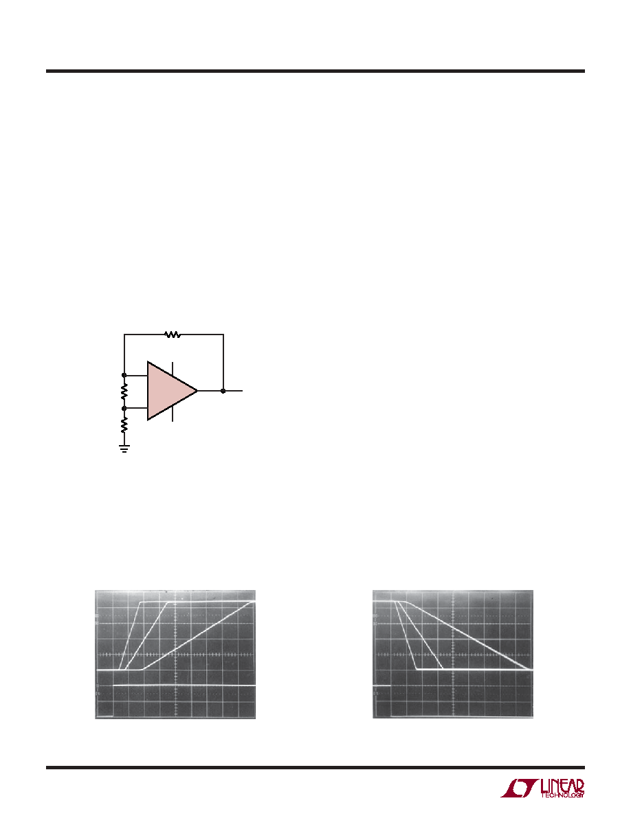
Comparator Applications
The single supply operation of the LT1006 and its ability to
swing close to ground while sinking current lends itself
to use as a precision comparator with TTL compatible
output.
Comparator Rise Response Time
to 10mV, 5mV, 2mV Overdrives
Comparator Fall Response Time
to 10mV, 5mV, 2mV Overdrives
Test Circuit for Offset Voltage and
Offset Drift with Temperature
–
+
V0
4.7V
– 0.3V
LT1006
50k*
*
**
RESISTORS MUST HAVE LOW
THERMOELECTRIC POTENTIAL.
THIS CIRCUIT IS ALSO USED AS
THE BURN-IN CONFIGURATION,
WITH SUPPLY VOLTAGES
INCREASED TO ± 20V
VO = 1000VOS
LT1006 TA04
100
50k*
0
VS = 5V, 0V
50s/DIV
1006 TA12a
0
2
4
OUTPUT (V)
INPUT (mV)
–100
0
VS = 5V, 0V
50s/DIV
1006 TA12b
0
2
4
OUTPUT (V)
INPUT (mV) –100
0
APPLICATIO S I FOR ATIO
WU
UU
相关PDF资料 |
PDF描述 |
|---|---|
| AD8039ARZ | IC OPAMP VF DUAL LP LN 8SOIC |
| KD1204PFS3 H | FAN 12VDC 40X10.5MM .7W 4.2CFM |
| LTC6800HMS8#PBF | IC INSTRUMENT AMP R-R I/O 8MSOP |
| KD1204PFS1 H | FAN 12VDC 40X10.5MM 1.4W 7.3CFM |
| OP27GPZ | IC OPAMP GP 8MHZ LN PREC 8DIP |
相关代理商/技术参数 |
参数描述 |
|---|---|
| LT1006D8 | 制造商:Micross Components, Inc. 功能描述:OP AMP, PRECISION, SINGLE SUPPLY - Bulk |
| LT1006MH | 制造商:Linear Technology 功能描述:OP Amp Single GP 44V 8-Pin TO-5 |
| LT1006MH/883 | 制造商:Linear Technology 功能描述:OP Amp Single GP 44V 8-Pin TO-5 |
| LT1006MJ8 | 制造商:Linear Technology 功能描述:OP Amp Single GP 44V 8-Pin CDIP |
| LT1006MJ8/883 | 制造商:Linear Technology 功能描述:Precision Single Op Amp Single/Dual-Supply |
发布紧急采购,3分钟左右您将得到回复。