- 您现在的位置:买卖IC网 > PDF目录79681 > LT1054CJ8#PBF (LINEAR TECHNOLOGY CORP) SWITCHED CAPACITOR REGULATOR, 40 kHz SWITCHING FREQ-MAX, CDSO8 PDF资料下载
参数资料
| 型号: | LT1054CJ8#PBF |
| 厂商: | LINEAR TECHNOLOGY CORP |
| 元件分类: | 稳压器 |
| 英文描述: | SWITCHED CAPACITOR REGULATOR, 40 kHz SWITCHING FREQ-MAX, CDSO8 |
| 封装: | 0.300 INCH, LEAD FREE, HERMETIC SEALED, CERAMIC, DIP-8 |
| 文件页数: | 13/16页 |
| 文件大小: | 264K |
| 代理商: | LT1054CJ8#PBF |
LT1054/LT1054L
6
1054lfg
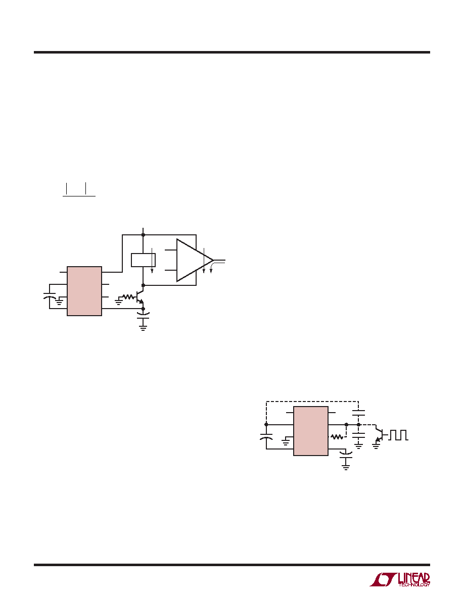
transistor must be added as shown in Figure 1. This will
prevent VOUT (Pin 5) from being pulled above the ground
pin (Pin 3) during start-up. Any small, general purpose
transistor such as 2N2222 or 2N2219 can be used. RX
should be chosen to provide enough base drive to the
external transistor so that it is saturated under nominal
output voltage and maximum output current conditions.
In some cases an N-channel enhancement mode MOSFET
can be used in place of the transistor.
RX ≤
VOUT
(
)β
IOUT
OSC (Pin 7): Oscillator Pin. This pin can be used to raise
or lower the oscillator frequency or to synchronize the
device to an external clock. Internally Pin 7 is connected
to the oscillator timing capacitor (Ct ≈ 150pF) which is
alternately charged and discharged by current sources of
±7A so that the duty cycle is ≈50%. The LT1054 oscillator
is designed to run in the frequency band where switch-
ing losses are minimized. However the frequency can be
raised, lowered, or synchronized to an external system
clock if necessary.
The frequency can be lowered by adding an external
capacitor (C1, Figure 2) from Pin 7 to ground. This will
increase the charge and discharge times which lowers the
oscillator frequency. The frequency can be increased by
adding an external capacitor (C2, Figure 2, in the range
of 5pF to 20pF) from Pin 2 to Pin 7. This capacitor will
couple charge into CT at the switch transitions, which will
shorten the charge and discharge time, raising the oscil-
lator frequency. Synchronization can be accomplished
by adding an external resistive pull-up from Pin 7 to the
reference pin (Pin 6). A 20k pull-up is recommended. An
open collector gate or an NPN transistor can then be used
to drive the oscillator pin at the external clock frequency
as shown in Figure 2. Pulling up Pin 7 to an external volt-
age is not recommended. For circuits that require both
frequency synchronization and regulation, an external
reference can be used as the reference point for the top
of the R1/R2 divider allowing Pin 6 to be used as a pull-
up point for Pin 7.
–
+
LOAD
CIN
COUT
LT1054 F01
IL
V+
RX
LT1054
FB/SHDN
CAP+
GND
CAP–
V+
OSC
VREF
VOUT
IQ
IOUT
+
VREF (Pin 6): Reference Output. This pin provides a 2.5V
reference point for use in LT1054-based regulator circuits.
The temperature coefficient of the reference voltage has
been adjusted so that the temperature coefficient of the
regulated output voltage is close to zero. This requires the
reference output to have a positive temperature coefficient
as can be seen in the typical performance curves. This
nonzero drift is necessary to offset a drift term inherent
in the internal reference divider and comparator network
tied to the feedback pin. The overall result of these drift
terms is a regulated output which has a slight positive
temperature coefficient at output voltages below 5V and a
slight negative TC at output voltages above 5V. Reference
output current should be limited, for regulator feedback
networks, to approximately 60A. The reference pin will
draw ≈100A when shorted to ground and will not af-
fect the internal reference/regulator, so that this pin can
also be used as a pull-up for LT1054 circuits that require
synchronization.
Figure 1
Figure 2
VIN
COUT
CIN
C2
C1
LT1054 F02
LT1054
FB/SHDN
CAP+
GND
CAP–
V+
OSC
VREF
VOUT
+
V+ (Pin 8): Input Supply. The LT1054 alternately charges
CIN to the input voltage when CIN is switched in parallel
with the input supply and then transfers charge to COUT
when CIN is switched in parallel with COUT. Switching oc-
curs at the oscillator frequency. During the time that CIN
PIN FUNCTIONS
相关PDF资料 |
PDF描述 |
|---|---|
| LM1501-7PV2H | 1-OUTPUT 50 W AC-DC REG PWR SUPPLY MODULE |
| LM1501-7RV3AHF | 1-OUTPUT 50 W AC-DC REG PWR SUPPLY MODULE |
| LM1601-7PV3AH | 1-OUTPUT 50 W AC-DC REG PWR SUPPLY MODULE |
| LM1601-7RV0AHF | 1-OUTPUT 50 W AC-DC REG PWR SUPPLY MODULE |
| LM1601-9RV3AHF | 1-OUTPUT 50 W AC-DC REG PWR SUPPLY MODULE |
相关代理商/技术参数 |
参数描述 |
|---|---|
| LT1054CN8 | 功能描述:IC REG SWITCHED CAP DBL INV 8DIP RoHS:否 类别:集成电路 (IC) >> PMIC - 稳压器 - DC DC 开关稳压器 系列:- 标准包装:2,500 系列:- 类型:升压(升压) 输出类型:可调式 输出数:1 输出电压:1.24 V ~ 30 V 输入电压:1.5 V ~ 12 V PWM 型:电流模式,混合 频率 - 开关:600kHz 电流 - 输出:500mA 同步整流器:无 工作温度:-40°C ~ 85°C 安装类型:表面贴装 封装/外壳:8-SOIC(0.154",3.90mm 宽) 包装:带卷 (TR) 供应商设备封装:8-SOIC |
| LT1054CN8#PBF | 功能描述:IC REG SWITCHED CAP DBL INV 8DIP RoHS:是 类别:集成电路 (IC) >> PMIC - 稳压器 - DC DC 开关稳压器 系列:- 标准包装:250 系列:- 类型:降压(降压) 输出类型:固定 输出数:1 输出电压:1.2V 输入电压:2.05 V ~ 6 V PWM 型:电压模式 频率 - 开关:2MHz 电流 - 输出:500mA 同步整流器:是 工作温度:-40°C ~ 85°C 安装类型:表面贴装 封装/外壳:6-UFDFN 包装:带卷 (TR) 供应商设备封装:6-SON(1.45x1) 产品目录页面:1032 (CN2011-ZH PDF) 其它名称:296-25628-2 |
| LT1054CN8PBF | 制造商:Linear Technology 功能描述:DC-DC converter,LT1054CN8 -Vin/2Vin 20mA |
| LT1054CP | 功能描述:电荷泵 Bipolar Regulated V RoHS:否 制造商:Maxim Integrated 功能:Inverting, Step Up 输出电压:- 1.5 V to - 5.5 V, 3 V to 11 V 输出电流:100 mA 电源电流:1 mA 最大工作温度:+ 70 C 封装 / 箱体:SOIC-8 Narrow 封装:Tube |
| LT1054CP | 制造商:Texas Instruments 功能描述:DC/DC Charge Pump Converter IC |
发布紧急采购,3分钟左右您将得到回复。