参数资料
| 型号: | LT1086CM-3.3#PBF |
| 厂商: | Linear Technology |
| 文件页数: | 9/16页 |
| 文件大小: | 0K |
| 描述: | IC REG LDO 3.3V 1.5A 3DD |
| 产品培训模块: | More Information on LDOs |
| 标准包装: | 50 |
| 稳压器拓扑结构: | 正,固定式 |
| 输出电压: | 3.3V |
| 输入电压: | 最高 20V |
| 电压 - 压降(标准): | 1.3V @ 1.5A |
| 稳压器数量: | 1 |
| 电流 - 输出: | 1.5A |
| 电流 - 限制(最小): | 1.5A |
| 工作温度: | 0°C ~ 150°C |
| 安装类型: | 表面贴装 |
| 封装/外壳: | TO-263-4,D²Pak(3 引线+接片),TO-263AA |
| 供应商设备封装: | D2PAK-3 |
| 包装: | 管件 |
| 产品目录页面: | 1325 (CN2011-ZH PDF) |
�� �
�
�LT1086� Series�
�APPLICATIO� N� S� I� N� FOR� M� ATIO� N�
�plugging� and� unplugging� in� the� system� will� not� generate�
�current� large� enough� to� do� any� damage.�
�The� adjustment� pin� can� be� driven� on� a� transient� basis�
�±� 25V,� with� respect� to� the� output� without� any� device�
�degradation.� Of� course� as� with� any� IC� regulator,� exceeding�
�the� maximum� input-to-output� voltage� differential� causes�
�the� internal� transistors� to� break� down� and� none� of� the�
�protection� circuitry� is� functional.�
�D1�
�1N4002�
�(OPTIONAL)�
�the� power� supply� may� need� to� be� cycled� down� to� zero� and�
�brought� up� again� to� make� the� output� recover.�
�Ripple� Rejection�
�For� the� LT1086� the� typical� curves� for� ripple� rejection�
�reflect� values� for� a� bypassed� adjust� pin.� This� curve� will� be�
�true� for� all� values� of� output� voltage.� For� proper� bypassing�
�and� ripple� rejection� approaching� the� values� shown,� the�
�impedance� of� the� adjust� pin� capacitor� at� the� ripple� fre-�
�quency� should� equal� the� value� of� R1,� (normally� 100� ?� to�
�120� ?� ).� The� size� of� the� required� adjust� pin� capacitor� is� a�
�V� IN�
�IN�
�LT1086� OUT�
�ADJ�
�+�
�C� ADJ�
�10� μ� F�
�R1�
�R2�
�+�
�V� OUT�
�C� OUT�
�150� μ� F�
�LT1086� ?� AI01�
�function� of� the� input� ripple� frequency.� At� 120Hz� the� adjust�
�pin� capacitor� should� be� 13� μ� F� if� R1� =� 100� ?� ;� at� 10kHz� only�
�0.16� μ� F� is� needed.�
�For� circuits� without� an� adjust� pin� bypass� capacitor� the�
�ripple� rejection� will� be� a� function� of� output� voltage.� The�
�output� ripple� will� increase� directly� as� a� ratio� of� the� output�
�Overload� Recovery�
�Like� any� of� the� IC� power� regulators,� the� LT1086� has� safe�
�area� protection.� The� safe� area� protection� decreases� the�
�current� limit� as� input-to-output� voltage� increases� and�
�keeps� the� power� transistor� inside� a� safe� operating� region�
�for� all� values� of� input-to-output� voltage.� The� LT1086�
�protection� is� designed� to� provide� some� output� current� at�
�all� values� of� input-to-output� voltage� up� to� the� device�
�breakdown.�
�When� power� is� first� turned� on,� as� the� input� voltage� rises,�
�the� output� follows� the� input,� allowing� the� regulator� to� start�
�up� into� very� heavy� loads.� During� the� start-up,� as� the� input�
�voltage� is� rising,� the� input-to-output� voltage� differential�
�remains� small,� allowing� the� regulator� to� supply� large�
�output� currents.� With� high� input� voltage,� a� problem� can�
�occur� wherein� removal� of� an� output� short� will� not� allow� the�
�output� voltage� to� recover.� Older� regulators� such� as� the�
�7800� series� also� exhibited� this� phenomenon,� so� it� is� not�
�unique� to� the� LT1086.�
�voltage� to� the� reference� voltage� (V� OUT� /V� REF� ).� For� ex-�
�ample,� with� the� output� voltage� equal� to� 5V� and� no� adjust�
�pin� capacitor,� the� output� ripple� will� be� higher� by� the� ratio�
�of� 5V/1.25V� or� four� times� larger.� Ripple� rejection� will� be�
�degraded� by� 12dB� from� the� value� shown� on� the� LT1086�
�curve.� Typical� curves� are� provided� for� the� 5V� and� 12V�
�devices� since� the� adjust� pin� is� not� available.�
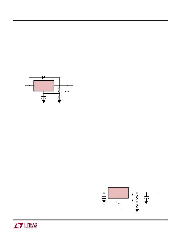
�Output� Voltage�
�The� LT1086� develops� a� 1.25V� reference� voltage� between�
�the� output� and� the� adjust� terminal� (see� Figure� 1).� By�
�placing� resistor� R1� between� these� two� terminals,� a� con-�
�stant� current� is� caused� to� flow� through� R1� and� down�
�through� R2� to� set� the� overall� output� voltage.� Normally� this�
�current� is� chosen� to� be� the� specified� minimum� load�
�current� of� 10mA.� Because� I� ADJ� is� very� small� and� constant�
�when� compared� with� the� current� through� R1,� it� repre-�
�sents� a� small� error� and� can� usually� be� ignored.� For� fixed�
�voltage� devices� R1� and� R2� are� included� in� the� device.�
�(�
�V� OUT� =� V� REF� 1� +� R2�
�The problem occurs with a heavy output load when the�
�input� voltage� is� high� and� the� output� voltage� is� low,� such� as�
�immediately� after� a� removal� of� a� short.� The� load� line� for�
�such� a� load� may� intersect� the� output� current� curve� at� two�
�points.� If� this� happens� there� are� two� stable� output� operat-�
�ing� points� for� the� regulator.� With� this� double� intersection�
�V� IN�
�IN� LT1086�
�ADJ�
�I� ADJ�
�50� μ� A�
�R1�
�)�
�OUT�
�V� REF�
�+� I� ADJ� R2�
�R1�
�R2�
�+�
�V� OUT�
�10� μ� F�
�TANTALUM�
�1086� ?� F01�
�Figure� 1.� Basic� Adjustable� Regulator�
�sn1086� 1086ffs�
�9�
�相关PDF资料 |
PDF描述 |
|---|---|
| 50USC10000MEFCSN30X40 | CAP ALUM 10000UF 50V 20% SNAP-IN |
| LT1529IQ-5#PBF | IC REG LDO 5V 3A DDPAK-5 |
| LT1529IQ-5 | IC REG LDO 5V 3A DDPAK-5 |
| EMM24DRUS | CONN EDGECARD 48POS DIP .156 SLD |
| RSA30DTKS | CONN EDGECARD 60POS DIP .125 SLD |
相关代理商/技术参数 |
参数描述 |
|---|---|
| LT1086CM36 | 制造商:LT 功能描述:New |
| LT1086CMPBF | 制造商:Linear Technology 功能描述:Voltage regulator,LT1086CM 23.5V |
| LT1086CT | 功能描述:IC REG LDO ADJ 1.5A TO220-3 RoHS:否 类别:集成电路 (IC) >> PMIC - 稳压器 - 线性 系列:- 产品培训模块:More Information on LDOs 标准包装:50 系列:- 稳压器拓扑结构:正,固定式 输出电压:3.3V 输入电压:最高 15V 电压 - 压降(标准):1.1V @ 800mA 稳压器数量:1 电流 - 输出:800mA 电流 - 限制(最小):800mA 工作温度:0°C ~ 125°C 安装类型:表面贴装 封装/外壳:TO-263-4,D²Pak(3 引线+接片),TO-263AA 供应商设备封装:D2PAK-3 包装:管件 |
| LT1086CT#PBF | 功能描述:IC REG LDO ADJ 1.5A TO220-3 RoHS:是 类别:集成电路 (IC) >> PMIC - 稳压器 - 线性 系列:- 标准包装:1 系列:- 稳压器拓扑结构:正,固定式 输出电压:8V 输入电压:10.5 V ~ 23 V 电压 - 压降(标准):1.7V @ 40mA 稳压器数量:1 电流 - 输出:100mA(最小值) 电流 - 限制(最小):- 工作温度:0°C ~ 125°C 安装类型:表面贴装 封装/外壳:8-SOIC(0.154",3.90mm 宽) 供应商设备封装:8-SOIC 包装:剪切带 (CT) 产品目录页面:1075 (CN2011-ZH PDF) 其它名称:296-24390-1 |
| LT1086CT12 | 制造商:Linear Technology 功能描述:IC V REG LDO +12V 1086 TO-220-3 |
发布紧急采购,3分钟左右您将得到回复。