- 您现在的位置:买卖IC网 > PDF目录14465 > LT1110CN8-12#PBF (Linear Technology)IC REG BUCK BOOST 12V 0.4A 8DIP PDF资料下载
参数资料
| 型号: | LT1110CN8-12#PBF |
| 厂商: | Linear Technology |
| 文件页数: | 6/16页 |
| 文件大小: | 0K |
| 描述: | IC REG BUCK BOOST 12V 0.4A 8DIP |
| 标准包装: | 50 |
| 类型: | 降压(降压),升压(升压) |
| 输出类型: | 固定 |
| 输出数: | 1 |
| 输出电压: | 12V |
| 输入电压: | 1 V ~ 30 V |
| 频率 - 开关: | 70kHz |
| 电流 - 输出: | 400mA |
| 同步整流器: | 无 |
| 工作温度: | 0°C ~ 70°C |
| 安装类型: | 通孔 |
| 封装/外壳: | 8-DIP(0.300",7.62mm) |
| 包装: | 管件 |
| 供应商设备封装: | 8-PDIP |
| 产品目录页面: | 1325 (CN2011-ZH PDF) |
�� �
�
�LT1110�
�LT1110� OPER� ATI�
�(�
�)�
�V� OUT� =� 220� mV� ?�
�+� 1� ?� .�
�?� R� 1�
�?�
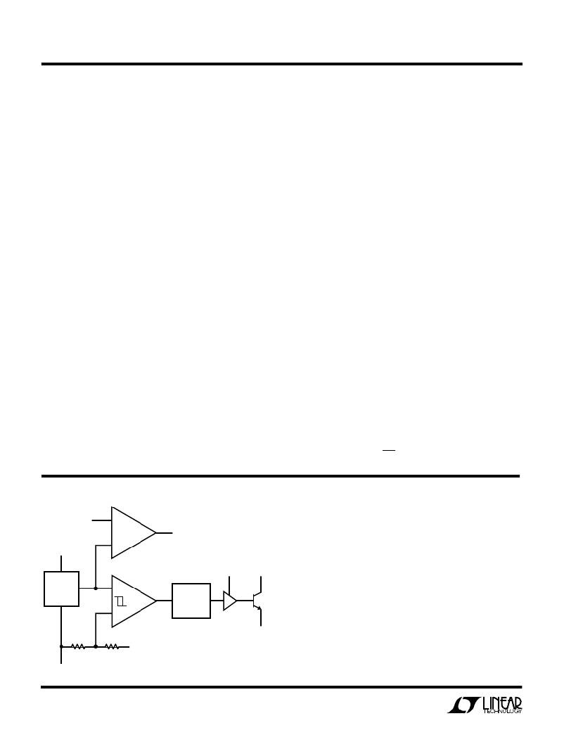
�The� LT1110� is� a� gated� oscillator� switcher.� This� type�
�architecture� has� very� low� supply� current� because� the�
�switch� is� cycled� only� when� the� feedback� pin� voltage� drops�
�below� the� reference� voltage.� Circuit� operation� can� best� be�
�understood� by� referring� to� the� LT1110� block� diagram�
�above.� Comparator� A1� compares� the� FB� pin� voltage� with�
�the� 220mV� reference� signal.� When� FB� drops� below�
�220mV,� A1� switches� on� the� 70kHz� oscillator.� The� driver�
�amplifier� boosts� the� signal� level� to� drive� the� output� NPN�
�power� switch� Q1.� An� adaptive� base� drive� circuit� senses�
�switch� current� and� provides� just� enough� base� drive� to�
�ensure� switch� saturation� without� overdriving� the� switch,�
�resulting� in� higher� efficiency.� The� switch� cycling� action�
�raises� the� output� voltage� and� FB� pin� voltage.� When� the� FB�
�voltage� is� sufficient� to� trip� A1,� the� oscillator� is� gated� off.� A�
�small� amount� of� hysteresis� built� into� A1� ensures� loop�
�stability� without� external� frequency� compensation.� When�
�the� comparator� is� low� the� oscillator� and� all� high� current�
�circuitry� is� turned� off,� lowering� device� quiescent� current� to�
�just� 300� μ� A� for� the� reference,� A1� and� A2.�
�The� oscillator� is� set� internally� for� 10� μ� s� ON� time� and� 5� μ� s�
�OFF� time,� optimizing� the� device� for� step-up� circuits� where�
�V� OUT� ≈� 3V� IN� ,� e.g.,� 1.5V� to� 5V.� Other� step-up� ratios� as� well�
�as� step-down� (buck)� converters� are� possible� at� slight�
�losses� in� maximum� achievable� power� output.�
�LT1110� -5,� -12� BLOCK� D� I� AGRA�
�A2� is� a� versatile� gain� block� that� can� serve� as� a� low� battery�
�detector,� a� linear� post� regulator,� or� drive� an� under� voltage�
�lockout� circuit.� The� negative� input� of� A2� is� internally�
�connected� to� the� 220mV� reference.� An� external� resistor�
�divider� from� V� IN� to� GND� provides� the� trip� point� for� A2.� The�
�AO� output� can� sink� 300� μ� A� (use� a� 47k� resistor� pull� up� to�
�+5V).� This� line� can� signal� a� microcontroller� that� the� battery�
�voltage� has� dropped� below� the� preset� level.� To� prevent� the�
�gain� block� from� operating� in� its� linear� region,� a� 2M� ?�
�resistor� can� be� connected� from� AO� to� SET.� This� provides�
�positive� feedback.�
�A� resistor� connected� between� the� I� LIM� pin� and� V� IN� adjusts�
�maximum� switch� current.� When� the� switch� current� ex-�
�ceeds� the� set� value,� the� switch� is� turned� off.� This� feature�
�is� especially� useful� when� small� inductance� values� are� used�
�with� high� input� voltages.� If� the� internal� current� limit� of� 1.5A�
�is� desired,� I� LIM� should� be� tied� directly� to� V� IN� .� Propagation�
�delay� through� the� current� limit� circuitry� is� about� 700ns.�
�In� step-up� mode,� SW2� is� connected� to� ground� and� SW1�
�drives� the� inductor.� In� step-down� mode,� SW1� is� con-�
�nected� to� V� IN� and� SW2� drives� the� inductor.� Output� voltage�
�is� set� by� the� following� equation� in� either� step-up� or� step-�
�down� modes� where� R1� is� connected� from� FB� to� GND� and�
�R2� is� connected� from� V� OUT� to� FB.�
�?� R 2� ?�
�(� 01� )�
�LT1110� -� -5,� -12� OPER� ATI�
�V� IN�
�SET�
�+�
�–�
�A2�
�AO�
�GAIN� BLOCK/ERROR� AMP�
�I� LIM�
�SW1�
�The� LT1110-5� and� LT1110-12� fixed� output� voltage� ver-�
�sions� have� the� gain� setting� resistors� on-chip.� Only� three�
�external� components� are� required� to� construct� a� 5V� or� 12V�
�output� converter.� 16� μ� A� flows� through� R1� and� R2� in� the�
�LT1110-5,� and� 39� μ� A� flows� in� the� LT1110-12.� This� current�
�220mV�
�REF�
�A1�
�COMPARATOR�
�OSCILLATOR�
�DRIVER�
�Q1�
�represents� a� load� and� the� converter� must� cycle� from� time�
�to� time� to� maintain� the� proper� output� voltage.� Output�
�ripple,� inherently� present� in� gated� oscillator� designs,� will�
�typically� run� around� 90mV� for� the� LT1110-5� and� 200mV�
�R1�
�R2�
�300k� ?�
�SENSE�
�LT1110-5:� R1� =� 13.8k� ?�
�LT1110-12:� R2� =� 5.6k� ?�
�SW2�
�for� the� LT1110-12� with� the� proper� inductor/capacitor�
�selection.� This� output� ripple� can� be� reduced� considerably�
�by� using� the� gain� block� amp� as� a� pre-amplifier� in� front� of�
�GND�
�6�
�LT1110� ?� BD02�
�the� FB� pin.� See� the� Applications� section� for� details.�
�相关PDF资料 |
PDF描述 |
|---|---|
| GCB40DHHR | CONN EDGECARD 80POS .050 DIP SLD |
| VI-BWT-EX-F2 | CONVERTER MOD DC/DC 6.5V 75W |
| VE-J0H-EX-B1 | CONVERTER MOD DC/DC 52V 75W |
| AYM06DTMD | CONN EDGECARD 12POS R/A .156 SLD |
| VI-J0B-EX-B1 | CONVERTER MOD DC/DC 95V 75W |
相关代理商/技术参数 |
参数描述 |
|---|---|
| LT1110CN8-5 | 功能描述:IC REG BUCK BOOST 5V 0.4A 8DIP RoHS:否 类别:集成电路 (IC) >> PMIC - 稳压器 - DC DC 开关稳压器 系列:- 标准包装:2,500 系列:- 类型:降压(降压) 输出类型:固定 输出数:1 输出电压:1.2V,1.5V,1.8V,2.5V 输入电压:2.7 V ~ 20 V PWM 型:- 频率 - 开关:- 电流 - 输出:50mA 同步整流器:是 工作温度:-40°C ~ 125°C 安装类型:表面贴装 封装/外壳:10-TFSOP,10-MSOP(0.118",3.00mm 宽)裸露焊盘 包装:带卷 (TR) 供应商设备封装:10-MSOP 裸露焊盘 |
| LT1110CN8-5#PBF | 功能描述:IC REG BUCK BOOST 5V 0.4A 8DIP RoHS:是 类别:集成电路 (IC) >> PMIC - 稳压器 - DC DC 开关稳压器 系列:- 标准包装:2,500 系列:- 类型:降压(降压) 输出类型:固定 输出数:1 输出电压:1.2V,1.5V,1.8V,2.5V 输入电压:2.7 V ~ 20 V PWM 型:- 频率 - 开关:- 电流 - 输出:50mA 同步整流器:是 工作温度:-40°C ~ 125°C 安装类型:表面贴装 封装/外壳:10-TFSOP,10-MSOP(0.118",3.00mm 宽)裸露焊盘 包装:带卷 (TR) 供应商设备封装:10-MSOP 裸露焊盘 |
| LT1110CS8 | 功能描述:IC REG BUCK BOOST ADJ 0.4A 8SOIC RoHS:否 类别:集成电路 (IC) >> PMIC - 稳压器 - DC DC 开关稳压器 系列:- 标准包装:2,500 系列:- 类型:降压(降压) 输出类型:固定 输出数:1 输出电压:1.2V,1.5V,1.8V,2.5V 输入电压:2.7 V ~ 20 V PWM 型:- 频率 - 开关:- 电流 - 输出:50mA 同步整流器:是 工作温度:-40°C ~ 125°C 安装类型:表面贴装 封装/外壳:10-TFSOP,10-MSOP(0.118",3.00mm 宽)裸露焊盘 包装:带卷 (TR) 供应商设备封装:10-MSOP 裸露焊盘 |
| LT1110CS8#PBF | 功能描述:IC REG BUCK BOOST ADJ 0.4A 8SOIC RoHS:是 类别:集成电路 (IC) >> PMIC - 稳压器 - DC DC 开关稳压器 系列:- 产品培训模块:MIC23xxx HyperLight Load™ Regulators 标准包装:5,000 系列:HyperLight Load® 类型:降压(降压) 输出类型:固定 输出数:1 输出电压:1.8V 输入电压:2.7 V ~ 5.5 V PWM 型:混合物 频率 - 开关:4MHz 电流 - 输出:2A 同步整流器:是 工作温度:-40°C ~ 125°C 安装类型:表面贴装 封装/外壳:8-VFDFN 裸露焊盘,8-MLF? 包装:带卷 (TR) 供应商设备封装:8-MLF?(2x2) 产品目录页面:1094 (CN2011-ZH PDF) 其它名称:576-3303-2 |
| LT1110CS8#TR | 功能描述:IC REG BUCK BOOST ADJ 0.4A 8SOIC RoHS:否 类别:集成电路 (IC) >> PMIC - 稳压器 - DC DC 开关稳压器 系列:- 标准包装:2,500 系列:- 类型:降压(降压) 输出类型:固定 输出数:1 输出电压:1.2V,1.5V,1.8V,2.5V 输入电压:2.7 V ~ 20 V PWM 型:- 频率 - 开关:- 电流 - 输出:50mA 同步整流器:是 工作温度:-40°C ~ 125°C 安装类型:表面贴装 封装/外壳:10-TFSOP,10-MSOP(0.118",3.00mm 宽)裸露焊盘 包装:带卷 (TR) 供应商设备封装:10-MSOP 裸露焊盘 |
发布紧急采购,3分钟左右您将得到回复。