- 您现在的位置:买卖IC网 > PDF目录14463 > LT1110CS8#PBF (Linear Technology)IC REG BUCK BOOST ADJ 0.4A 8SOIC PDF资料下载
参数资料
| 型号: | LT1110CS8#PBF |
| 厂商: | Linear Technology |
| 文件页数: | 11/16页 |
| 文件大小: | 0K |
| 描述: | IC REG BUCK BOOST ADJ 0.4A 8SOIC |
| 标准包装: | 100 |
| 类型: | 降压(降压),升压(升压) |
| 输出类型: | 可调式 |
| 输出数: | 1 |
| 输出电压: | 可调 |
| 输入电压: | 1 V ~ 30 V |
| 频率 - 开关: | 70kHz |
| 电流 - 输出: | 400mA |
| 同步整流器: | 无 |
| 工作温度: | 0°C ~ 70°C |
| 安装类型: | 表面贴装 |
| 封装/外壳: | 8-SOIC(0.154",3.90mm 宽) |
| 包装: | 管件 |
| 供应商设备封装: | 8-SOIC |
�� �
�
�LT1110�
�A� PPLICATI�
�S� I� FOR� ATIO�
�dissipation� inside� the� LT1110.� Output� voltage� is� deter-�
�mined� by�
�Converter”� section� with� the� following� conservative� ex-�
�pression� for� V� SW� :�
�V� OUT� =� ?� 1� +�
�(�
�)�
�R� 1� ?�
�?�
�?�
�R� 2� ?�
�?� 220� mV� .�
�(� 23� )�
�V� SW� =� V� R� 1� +� V� SAT� ≈� 0� .� 9� V� .� (� 24� )�
�R2� provides� a� current� path� to� turn� off� Q1.� R3� provides� base�
�R3� programs� switch� current� limit.� This� is� especially� im-�
�portant� in� applications� where� the� input� varies� over� a� wide�
�range.� Without� R3,� the� switch� stays� on� for� a� fixed� time�
�each� cycle.� Under� certain� conditions� the� current� in� L1� can�
�build� up� to� excessive� levels,� exceeding� the� switch� rating�
�and/or� saturating� the� inductor.� The� 220� ?� resistor� pro-�
�grams� the� switch� to� turn� off� when� the� current� reaches�
�approximately� 800mA.� When� using� the� LT1110� in� step-�
�down� mode,� output� voltage� should� be� limited� to� 6.2V� or�
�less.� Higher� output� voltages� can� be� accommodated� by�
�inserting� a� 1N5818� diode� in� series� with� the� SW2� pin�
�(anode� connected� to� SW2).�
�drive� to� Q1.� R4� and� R5� set� output� voltage.�
�Inverting� Configurations�
�The� LT1110� can� be� configured� as� a� positive-to-negative�
�converter� (Figure� 7),� or� a� negative-to-positive� converter�
�(Figure� 8).� In� Figure� 7,� the� arrangement� is� very� similar� to�
�a� step-down,� except� that� the� high� side� of� the� feedback� is�
�referred� to� ground.� This� level� shifts� the� output� negative.� As�
�in� the� step-down� mode,� D1� must� be� a� Schottky� diode,�
�and� ?� V� OUT� ?� should� be� less� than� 6.2V.� More� negative� out-�
�put� voltages� can� be� accommodated� as� in� the� prior� section.�
�+V� IN�
�R3�
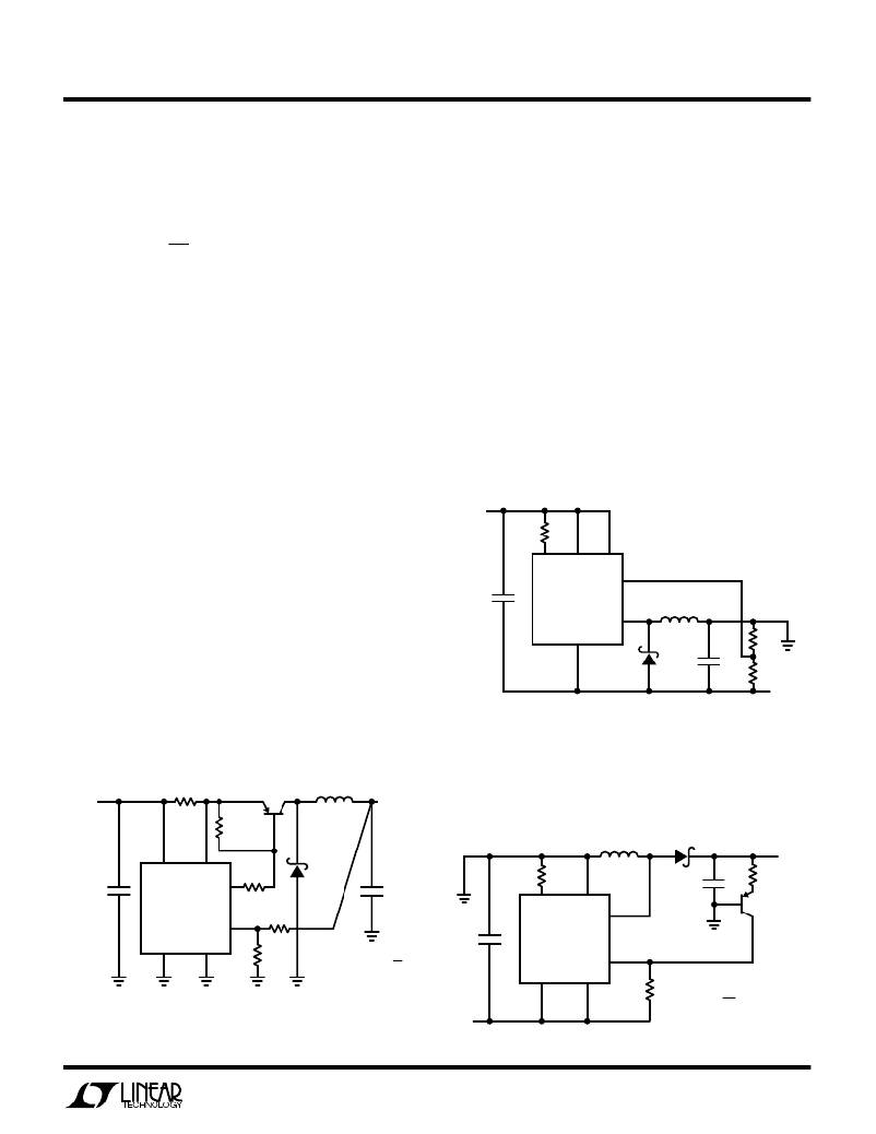
�Higher� Current� Step-Down� Operation�
�Output� current� can� be� increased� by� using� a� discrete� PNP�
�pass� transistor� as� shown� in� Figure� 6.� R1� serves� as� a�
�+�
�C2�
�I� LIM�
�V� IN�
�LT1110�
�SW1�
�FB�
�current� limit� sense.� When� the� voltage� drop� across� R1�
�SW2�
�L1�
�equals� a� V� BE� ,� the� switch� turns� off.� For� temperature� com-�
�pensation� a� Schottky� diode� can� be� inserted� in� series� with�
�GND�
�D1�
�1N5818�
�+�
�C1�
�R1�
�the� I� LIM� pin.� This� also� lowers� the� maximum� drop� across� R1�
�to� V� BE� –� V� D� ,� increasing� efficiency.� As� shown,� switch�
�current� is� limited� to� 2A.� Inductor� value� can� be� calculated�
�based� on� formulas� in� the� “Inductor� Selection� Step-Down�
�Q1�
�R2�
�–V� OUT�
�LT1110� ?� TA03�
�Figure� 7.� Positive-to-Negative� Converter�
�In� Figure� 8,� the� input� is� negative� while� the� output� is�
�positive.� In� this� configuration,� the� magnitude� of� the� input�
�V� IN�
�25V�
�R1�
�0.3� ?�
�MJE210� OR�
�ZETEX� ZTX789A�
�L1�
�V� OUT�
�voltage� can� be� higher� or� lower� than� the� output� voltage.� A�
�level� shift,� provided� by� the� PNP� transistor,� supplies� proper�
�MAX�
�R2�
�220�
�polarity� feedback� information� to� the� regulator.�
�L1� D1�
�C2�
�+�
�V� IN�
�I� L�
�SW1�
�R3�
�330�
�D1�
�1N5821�
�+�
�C1�
�+�
�C1�
�R1�
�+V� OUT�
�LT1110�
�I� LIM�
�V� IN�
�2N3906�
�(�
�GND�
�SW2�
�FB�
�R4�
�R5�
�V� OUT� =� 220mV�
�R4�
�1� +� R5�
�)�
�+�
�C2�
�AO�
�LT1110�
�SW1�
�FB�
�GND�
�SW2�
�LT1110� ?� TA16�
�Figure� 6.� Q1� Permits� Higher-Current� Switching.�
�–V� IN�
�R2�
�V� OUT� =�
�(� R1R2� )� 220mV� +� 0.6V�
�LT1110� ?� TA04�
�LT1110� Functions� as� Controller.�
�Figure� 8.� Negative-to-Positive� Converter�
�11�
�相关PDF资料 |
PDF描述 |
|---|---|
| LT3990IMSE-5#PBF | IC REG BUCK ADJ 0.35A 16MSOP |
| VE-BWD-EW-F4 | CONVERTER MOD DC/DC 85V 100W |
| LT3990IMSE-3.3#PBF | IC REG BUCK ADJ 0.35A 16MSOP |
| LT3971EMSE16#PBF | IC REG BUCK ADJ 1.2A 16MSOP |
| LTC3423EMS | IC REG BOOST SYNC ADJ 1A 10MSOP |
相关代理商/技术参数 |
参数描述 |
|---|---|
| LT1111 | 制造商:LINER 制造商全称:Linear Technology 功能描述:Micropower DC/DC Converter Adjustable and Fixed 5V, 12V |
| LT1111_03 | 制造商:LINER 制造商全称:Linear Technology 功能描述:Micropower DC/DC Converter Adjustable and Fixed 5V, 12V |
| LT1111-12 | 制造商:LINER 制造商全称:Linear Technology 功能描述:Micropower DC/DC Converter Adjustable and Fixed 5V, 12V |
| LT1111-5 | 制造商:LINER 制造商全称:Linear Technology 功能描述:Micropower DC/DC Converter Adjustable and Fixed 5V, 12V |
| LT1111C | 制造商:LINER 制造商全称:Linear Technology 功能描述:Micropower DC/DC Converter Adjustable and Fixed 5V, 12V |
发布紧急采购,3分钟左右您将得到回复。