- 您现在的位置:买卖IC网 > PDF目录1821 > LT1111IS8#TRPBF (Linear Technology)IC REG BUCK BOOST INV ADJ 8SOIC PDF资料下载
参数资料
| 型号: | LT1111IS8#TRPBF |
| 厂商: | Linear Technology |
| 文件页数: | 12/16页 |
| 文件大小: | 0K |
| 描述: | IC REG BUCK BOOST INV ADJ 8SOIC |
| 标准包装: | 2,500 |
| 类型: | 降压(降压),升压(升压),反相 |
| 输出类型: | 可调式 |
| 输出数: | 1 |
| 输出电压: | 可调 |
| 输入电压: | 2 V ~ 30 V |
| 频率 - 开关: | 72kHz |
| 电流 - 输出: | 400mA |
| 同步整流器: | 无 |
| 工作温度: | -40°C ~ 105°C |
| 安装类型: | 表面贴装 |
| 封装/外壳: | 8-SOIC(0.154",3.90mm 宽) |
| 包装: | 带卷 (TR) |
| 供应商设备封装: | 8-SOIC |
�� �
�
�LT1111�
�A� PPLICATI�
�S� I� FOR� ATIO�
�L1�
�D1�
�+�
�C1�
�R1�
�V� OUT�
�I� L�
�I� LIM�
�V� IN�
�2N3906�
�+�
�C2�
�LT1111�
�SW1�
�(� )�
�V� OUT� =� 1.25V� +� 0.6V�
�–V� IN�
�A0�
�GND�
�FB�
�SW2�
�R2�
�LT1111� ?� F08�
�R1�
�R2�
�SWITCH�
�ON�
�OFF�
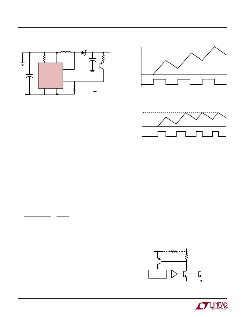
�Figure� 9.� No� Current� Limit� Causes� Large� Inductor�
�LT1111� ?� F09�
�Current� Build-Up�
�Figure� 8.� Negative-to-Positive� Converter�
�Using� the� I� LIM� Pin�
�The� LT1111� switch� can� be� programmed� to� turn� off� at� a� set�
�switch� current,� a� feature� not� found� on� competing� devices.�
�I� L�
�PROGRAMMED� CURRENT� LIMIT�
�This� enables� the� input� to� vary� over� a� wide� range� without�
�exceeding� the� maximum� switch� rating� or� saturating� the�
�SWITCH�
�ON�
�OFF�
�LT1111� ?� F10�
�inductor.� Consider� the� case� wh� ere� analysis� shows� the�
�LT1111� must� operate� at� an� 800mA� peak� switch� current�
�with� a� 2V� input.� If� V� IN� rises� to� 4V,� the� peak� switch� current�
�will� rise� to� 1.6A,� exceeding� the� maximum� switch� current�
�rating.� With� the� proper� resistor� selected� (see� the� “Maxi-�
�mum� Switch� Current� vs� I� LIM� ”� characteristic),� the� switch�
�current� will� be� limited� to� 800mA,� even� if� the� input� voltage�
�increases.�
�Another� situation� where� the� I� LIM� feature� is� useful� occurs�
�when� the� device� goes� into� continuous� mode� operation.�
�This� occurs� in� step-up� mode� when:�
�Figure� 10.� Current� Limit� Keeps� Inductor� Current� Under� Control�
�Figure� 11� details� current� limit� circuitry.� Sense� transistor�
�Q1,� whose� base� and� emitter� are� paralleled� with� power�
�switch� Q2,� is� ratioed� such� that� approximately� 0.5%� of� Q2’s�
�collector� current� flows� in� Q1’s� collector.� This� current� is�
�passed� through� internal� 80� ?� resistor� R1� and� out� through�
�the� I� LIM� pin.� The� value� of� the� external� resistor� connected�
�between� I� LIM� and� V� IN� sets� the� current� limit.� When� suffi-�
�cient� switch� current� flows� to� develop� a� V� BE� across� R1� +�
�R� LIM� ,� Q3� turns� on� and� injects� current� into� the� oscillator,�
�V� OUT� +� V� DIODE�
�V� IN� ?� V� SW�
�<�
�1�
�1� ?� DC�
�(� 25� )�
�turning� off� the� switch.� Delay� through� this� circuitry� is�
�approximately� 1� μ� s.� The� current� trip� point� becomes� less�
�accurate� for� switch� ON� times� less� than� 3� μ� s.� Resistor�
�values� programming� switch� ON� time� for� 1� μ� s� or� less� will�
�When� the� input� and� output� voltages� satisfy� this� relation-�
�ship,� inductor� current� does� not� go� to� zero� during� the�
�cause� spurious� response� in� the� switch� circuitry� although�
�the� device� will� still� maintain� output� regulation.�
�switch� OFF� time.� When� the� switch� turns� on� again,� the�
�current� ramp� starts� from� the� non-zero� current� level� in� the�
�R� LIM�
�(EXTERNAL)�
�I� LIM�
�inductor� just� prior� to� switch� turn-on.� As� shown� in� Figure�
�9,� the� inductor� current� increases� to� a� high� level� before� the�
�comparator� turns� off� the� oscillator.� This� high� current� can�
�cause� excessive� output� ripple� and� requires� oversizing� the�
�output� capacitor� and� inductor.� With� the� I� LIM� feature,�
�however,� the� switch� current� turns� off� at� a� programmed�
�level� as� shown� in� Figure� 10,� keeping� output� ripple� to� a�
�V� IN�
�Q3�
�OSCILLATOR�
�DRIVER�
�R1�
�80� ?�
�(INTERNAL)�
�SW1�
�Q1�
�Q2�
�SW2�
�LT1111� ?� F11�
�minimum.�
�12�
�Figure� 11.� LT1111� Current� Limit� Circuitry�
�1111fd�
�相关PDF资料 |
PDF描述 |
|---|---|
| LT1117IST-5#TR | IC REG LDO 5V .8A SOT-223 |
| LT1118CS8-2.85 | IC REG LDO 2.85V .8A 8SOIC |
| LT1120IS8#TRPBF | IC REG LDO ADJ 125MA 8SOIC |
| LT1121AIS8 | IC REG LDO ADJ .15A 8-SOIC |
| LT1129MPST-3.3#TRPBF | IC REG LDO 3.3V .7A SOT223 |
相关代理商/技术参数 |
参数描述 |
|---|---|
| LT1111M | 制造商:LINER 制造商全称:Linear Technology 功能描述:Micropower DC/DC Converter Adjustable and Fixed 5V, 12V |
| LT1111MJ8 | 制造商:LINER 制造商全称:Linear Technology 功能描述:Micropower DC/DC Converter Adjustable and Fixed 5V, 12V |
| LT1111MJ8-12 | 制造商:LINER 制造商全称:Linear Technology 功能描述:Micropower DC/DC Converter Adjustable and Fixed 5V, 12V |
| LT1111MJ8-5 | 制造商:LINER 制造商全称:Linear Technology 功能描述:Micropower DC/DC Converter Adjustable and Fixed 5V, 12V |
| LT1112 | 制造商:LINEAR 制造商全称:LINEAR 功能描述:Dual/Quad Low Power Precision, Picoamp Input Op Amps |
发布紧急采购,3分钟左右您将得到回复。