参数资料
| 型号: | LT1121IN8-3.3 |
| 厂商: | Linear Technology |
| 文件页数: | 9/16页 |
| 文件大小: | 0K |
| 描述: | IC REG LDO 3.3V .15A 8-DIP |
| 标准包装: | 50 |
| 稳压器拓扑结构: | 正,固定式 |
| 输出电压: | 3.3V |
| 输入电压: | 4.17 V ~ 30 V |
| 电压 - 压降(标准): | 0.42V @ 150mA |
| 稳压器数量: | 1 |
| 电流 - 输出: | 150mA |
| 工作温度: | -40°C ~ 125°C |
| 安装类型: | 通孔 |
| 封装/外壳: | 8-DIP(0.300",7.62mm) |
| 供应商设备封装: | 8-PDIP |
| 包装: | 管件 |
�� ��
��
��LT1121/LT1121-3.3/LT1121-5�
�APPLICATIONS� INFORMATION�
�?� ?� 3.75V� ?� ?� ?� (� –12mV� )� =� (� –38mV� )�
�R2�
�(� )�
�(�
�)�
�V� OUT� =� 3.75V� 1� +� +� I� ADJ� ?� R2�
�TheLT1121isamicropowerlowdropoutregulatorwith�
�shutdown,� capable� of� supplying� up� to� 150mA� of� output�
�current� at� a� dropout� voltage� of� 0.4V.� The� device� operates�
�with� very� low� quiescent� current� (30μA).� In� shutdown� the�
�quiescent� current� drops� to� only� 16μA.� In� addition� to� the�
�low� quiescent� current� the� LT1121� incorporates� several�
�protection� features� which� make� it� ideal� for� use� in� battery-�
�powered� systems.� The� device� is� protected� against� both�
�reverse� input� voltages� and� reverse� output� voltages.� In�
�battery� backup� applications� where� the� output� can� be� held�
�up� by� a� backup� battery� when� the� input� is� pulled� to� ground,�
�the� LT1121� acts� like� it� has� a� diode� in� series� with� its� output�
�and� prevents� reverse� current� flow.�
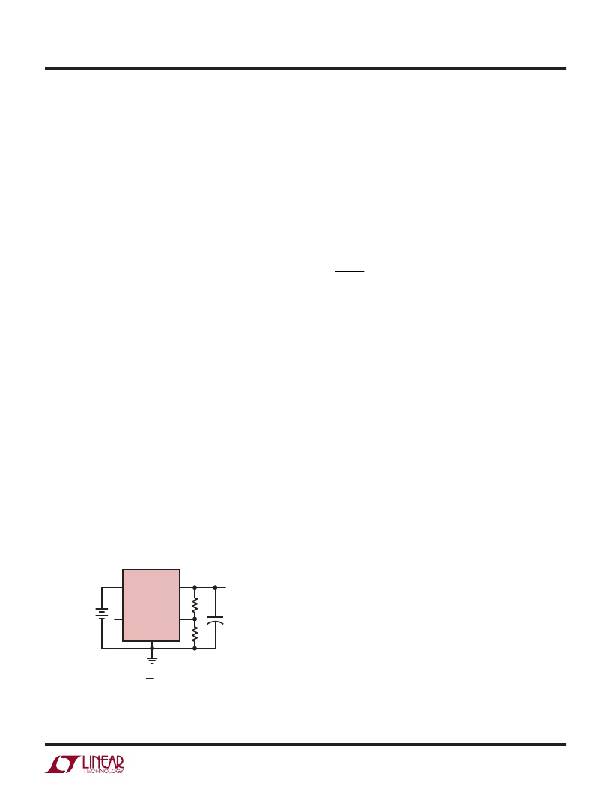
�Adjustable� Operation�
�The� adjustable� version� of� the� LT1121� has� an� output� voltage�
�range� of� 3.75V� to� 30V.� The� output� voltage� is� set� by� the�
�ratio� of� two� external� resistors� as� shown� in� Figure� 1.� The�
�device� servos� the� output� voltage� to� maintain� the� voltage�
�at� the� adjust� pin� at� 3.75V.� The� current� in� R1� is� then� equal�
�to� 3.75V/R1.� The� current� in� R2� is� equal� to� the� sum� of� the�
�current� in� R1� and� the� adjust� pin� bias� current.� The� adjust�
�pin� bias� current,� 150nA� at� 25°C,� flows� through� R2� into� the�
�adjust� pin.� The� output� voltage� can� be� calculated� according�
�to� the� formula� in� Figure� 1.� The� value� of� R1� should� be� less�
�than� 400k� to� minimize� errors� in� the� output� voltage� caused�
�by� the� adjust� pin� bias� current.� Note� that� in� shutdown� the�
�output� is� turned� off� and� the� divider� current� will� be� zero.�
�Curves� of� Adjust� Pin� Voltage� vs� Temperature� and� Adjust�
�Pin� Bias� Current� vs� Temperature� appear� in� the� Typical�
�Performance� Characteristics.� The� reference� voltage� at� the�
�adjust� pin� has� a� slight� positive� temperature� coefficient� of�
�IN� OUT� V� OUT�
�LT1121�
�+�
�SHDN� ADJ�
�GND� R1�
�1121� ?� F01�
�R2�
�R1�
�V� ADJ� =� 3.75V�
�I� ADJ� =� 150nA� AT� 25� °� C�
�OUTPUT� RANGE� =� 3.75V� TO� 30V�
�Figure� 1.� Adjustable� Operation�
�approximately� 15ppm/°C.� The� adjust� pin� bias� current� has�
�a� negative� temperature� coefficient.� These� effects� are� small�
�and� will� tend� to� cancel� each� other.�
�The� adjustable� device� is� specified� with� the� adjust� pin� tied�
�to� the� output� pin.� This� sets� the� output� voltage� to� 3.75V.�
�Specifications� for� output� voltage� greater� than� 3.75V� will�
�be� proportional� to� the� ratio� of� the� desired� output� voltage�
�to� 3.75V� (V� OUT� /3.75V).� For� example:� load� regulation� for� an�
�output� current� change� of� 1mA� to� 150mA� is� –12mV� typical�
�at� V� OUT� =� 3.75V.� At� V� OUT� =� 12V,� load� regulation� would� be:�
�?� 12V� ?�
�Thermal� Considerations�
�Power� handling� capability� will� be� limited� by� maximum�
�rated� junction� temperature� (125°C).� Power� dissipated� by�
�the� device� will� be� made� up� of� two� components:�
�1.� Output� current� multiplied� by� the� input/output� voltage�
�differential:� I� OUT� ?� (� V� IN� –� V� OUT� ),� and�
�2.� Ground� pin� current� multiplied� by� the� input� voltage:�
�I� GND� ?� V� IN� .�
�The� ground� pin� current� can� be� found� by� examining� the�
�Ground� Pin� Current� curves� in� the� Typical� Performance�
�Characteristics.� Power� dissipation� will� be� equal� to� the�
�sum� of� the� two� components� listed� above.�
�The� LT1121� series� regulators� have� internal� thermal� limiting�
�designed� to� protect� the� device� during� overload� conditions.�
�For� continuous� normal� load� conditions� the� maximum� junc-�
�tion� temperature� rating� of� 125°C� must� not� be� exceeded.�
�It� is� important� to� give� careful� consideration� to� all� sources�
�of� thermal� resistance� from� junction� to� ambient.� Additional�
�heat� sources� mounted� nearby� must� also� be� considered.�
�Heat� sinking,� for� surface� mount� devices,� is� accomplished�
�by� using� the� heat� spreading� capabilities� of� the� PC� board�
�and� its� copper� traces.� Copper� board� stiffeners� and� plated�
�through� holes� can� also� be� used� to� spread� the� heat� gener-�
�ated� by� power� devices.� Tables� 1� through� 5� list� thermal�
�resistances� for� each� package.� Measured� values� of� thermal�
�resistance� for� several� different� board� sizes� and� copper�
�areas� are� listed� for� each� package.� All� measurements� were�
�taken� in� still� air,� on� 3/32"� FR-4� board� with� 1oz� copper.� All�
�1121fg�
�9�
�相关PDF资料 |
PDF描述 |
|---|---|
| LT1121IN8#PBF | IC REG LDO ADJ .15A 8-DIP |
| HMM22DRYN-S13 | CONN EDGECARD 44POS .156 EXTEND |
| NCP4587DMX18TCG | IC REG LDO 1.8V .15A 6-XDFN |
| HSM22DRYH-S13 | CONN EDGECARD 44POS .156 EXTEND |
| GCC65DRES-S734 | CONN EDGECARD 130PS .100 EYELET |
相关代理商/技术参数 |
参数描述 |
|---|---|
| LT1121IN8-5 | 功能描述:IC REG LDO 5V .15A 8-DIP RoHS:否 类别:集成电路 (IC) >> PMIC - 稳压器 - 线性 系列:- 标准包装:3,000 系列:- 稳压器拓扑结构:正,固定式 输出电压:3V 输入电压:最高 5.5V 电压 - 压降(标准):0.12V @ 150mA 稳压器数量:1 电流 - 输出:150mA(最小值) 电流 - 限制(最小):220mA 工作温度:-40°C ~ 125°C 安装类型:表面贴装 封装/外壳:SOT-23-5 细型,TSOT-23-5 供应商设备封装:TSOT-23-5 包装:带卷 (TR) 其它名称:ADP160AUJZ-3.0-R7TR |
| LT1121IN8-5#PBF | 功能描述:IC REG LDO 5V .15A 8-DIP RoHS:是 类别:集成电路 (IC) >> PMIC - 稳压器 - 线性 系列:- 产品培训模块:MIC5365/66 Ultra-small LDO Regulators 标准包装:1 系列:- 稳压器拓扑结构:正,固定式 输出电压:3V 输入电压:最高 5.5V 电压 - 压降(标准):0.155V @ 150mA 稳压器数量:1 电流 - 输出:150mA 电流 - 限制(最小):200mA 工作温度:-40°C ~ 125°C 安装类型:表面贴装 封装/外壳:4-UDFN 裸露焊盘,4-TMLF? 供应商设备封装:4-TMLF?(1x1) 包装:Digi-Reel® 其它名称:576-3192-6 |
| LT1121IS8 | 功能描述:IC REG LDO ADJ .15A 8-SOIC RoHS:否 类别:集成电路 (IC) >> PMIC - 稳压器 - 线性 系列:- 产品培训模块:More Information on LDOs 标准包装:50 系列:- 稳压器拓扑结构:正,固定式 输出电压:3.3V 输入电压:最高 15V 电压 - 压降(标准):1.1V @ 800mA 稳压器数量:1 电流 - 输出:800mA 电流 - 限制(最小):800mA 工作温度:0°C ~ 125°C 安装类型:表面贴装 封装/外壳:TO-263-4,D²Pak(3 引线+接片),TO-263AA 供应商设备封装:D2PAK-3 包装:管件 |
| LT1121IS8#PBF | 功能描述:IC REG LDO ADJ .15A 8-SOIC RoHS:是 类别:集成电路 (IC) >> PMIC - 稳压器 - 线性 系列:- 标准包装:1 系列:- 稳压器拓扑结构:正,固定式 输出电压:8V 输入电压:10.5 V ~ 23 V 电压 - 压降(标准):1.7V @ 40mA 稳压器数量:1 电流 - 输出:100mA(最小值) 电流 - 限制(最小):- 工作温度:0°C ~ 125°C 安装类型:表面贴装 封装/外壳:8-SOIC(0.154",3.90mm 宽) 供应商设备封装:8-SOIC 包装:剪切带 (CT) 产品目录页面:1075 (CN2011-ZH PDF) 其它名称:296-24390-1 |
| LT1121IS8#PBF | 制造商:Linear Technology 功能描述:Linear Voltage Regulator IC |
发布紧急采购,3分钟左右您将得到回复。