- 您现在的位置:买卖IC网 > PDF目录5768 > LT1167ACS8#PBF (Linear Technology)IC PREC INSTRMNT-AMP PROG 8-SOIC PDF资料下载
参数资料
| 型号: | LT1167ACS8#PBF |
| 厂商: | Linear Technology |
| 文件页数: | 5/22页 |
| 文件大小: | 0K |
| 描述: | IC PREC INSTRMNT-AMP PROG 8-SOIC |
| 标准包装: | 100 |
| 放大器类型: | 仪表 |
| 电路数: | 1 |
| 转换速率: | 1.2 V/µs |
| 增益带宽积: | 1MHz |
| 电流 - 输入偏压: | 50pA |
| 电压 - 输入偏移: | 15µV |
| 电流 - 电源: | 900µA |
| 电流 - 输出 / 通道: | 27mA |
| 电压 - 电源,单路/双路(±): | 4.6 V ~ 36 V,±2.3 V ~ 18 V |
| 工作温度: | 0°C ~ 70°C |
| 安装类型: | 表面贴装 |
| 封装/外壳: | 8-SOIC(0.154",3.90mm 宽) |
| 供应商设备封装: | 8-SO |
| 包装: | 管件 |
| 产品目录页面: | 1323 (CN2011-ZH PDF) |
LT1167
13
1167fc
THEORY OF OPERATION
Input and Output Offset Voltage
The offset voltage of the LT1167 has two components:
the output offset and the input offset. The total offset
voltage referred to the input (RTI) is found by dividing the
output offset by the programmed gain (G) and adding it
to the input offset. At high gains the input offset voltage
dominates, whereas at low gains the output offset voltage
dominates. The total offset voltage is:
Total input offset voltage (RTI)
= input offset + (output offset/G)
Total output offset voltage (RTO)
= (input offset G) + output offset
Reference Terminal
The reference terminal is one end of one of the four 10k
resistors around the difference amplifier. The output volt-
age of the LT1167 (Pin 6) is referenced to the voltage on
the reference terminal (Pin 5). Resistance in series with
the REF pin must be minimized for best common mode
rejection. For example, a 2Ω resistance from the REF pin
to ground will not only increase the gain error by 0.02%
but will lower the CMRR to 80dB.
Single Supply Operation
For single supply operation, the REF pin can be at the
same potential as the negative supply (Pin 4) provided the
output of the instrumentation amplifier remains inside the
specified operating range and that one of the inputs is at
least 2.5V above ground. The barometer application on
the front page of this data sheet is an example that satis-
fies these conditions. The resistance Rb from the bridge
transducer to ground sets the operating current for the
bridge and also has the effect of raising the input common
mode voltage. The output of the LT1167 is always inside
the specified range since the barometric pressure rarely
goes low enough to cause the output to rail (30.00 inches
of Hg corresponds to 3.000V). For applications that require
the output to swing at or below the REF potential, the
voltage on the REF pin can be level shifted. An op amp is
used to buffer the voltage on the REF pin since a parasitic
series resistance will degrade the CMRR. The application
in the back of this data sheet, Four Digit Pressure Sensor,
is an example.
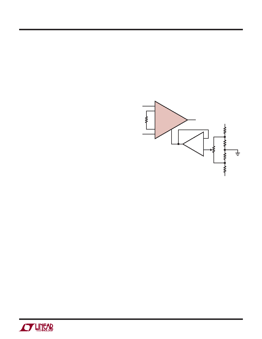
Output Offset Trimming
The LT1167 is laser trimmed for low offset voltage so that
no external offset trimming is required for most applica-
tions. In the event that the offset needs to be adjusted, the
circuit in Figure 2 is an example of an optional offset adjust
circuit. The op amp buffer provides a low impedance to
the REF pin where resistance must be kept to minimum
for best CMRR and lowest gain error.
–
+
2
–IN
OUTPUT
+IN
1
8
10k
100Ω
–10mV
1167 F02
V–
V+
10mV
5
2
3
1
6
1/2
LT1112
±10mV
ADJUSTMENT RANGE
RG
3
–
+
LT1167
REF
Figure 2. Optional Trimming of Output Offset Voltage
Input Bias Current Return Path
The low input bias current of the LT1167 (350pA) and
the high input impedance (200GΩ) allow the use of high
impedance sources without introducing additional offset
voltage errors, even when the full common mode range is
required. However, a path must be provided for the input
bias currents of both inputs when a purely differential
signal is being amplified. Without this path the inputs
will float to either rail and exceed the input common
mode range of the LT1167, resulting in a saturated input
stage. Figure 3 shows three examples of an input bias
current path. The first example is of a purely differential
signal source with a 10kΩ input current path to ground.
Since the impedance of the signal source is low, only one
resistor is needed. Two matching resistors are needed for
higher impedance signal sources as shown in the second
example. Balancing the input impedance improves both
common mode rejection and DC offset. The need for input
resistors is eliminated if a center tap is present as shown
in the third example.
相关PDF资料 |
PDF描述 |
|---|---|
| 3-644757-3 | CONN HEADER 3POS VERT .156 GOLD |
| LT1167ACS8 | IC PREC INSTRMNT-AMP PROG 8-SOIC |
| LT1079ISW#TR | IC OPAMP PREC QUAD MCRPWR 16SOIC |
| 3-644757-2 | CONN HEADER 2POS VERT .156 GOLD |
| LT1167ACN8#PBF | IC PREC INSTRMNT-AMP PROG 8-DIP |
相关代理商/技术参数 |
参数描述 |
|---|---|
| LT1167AI | 制造商:LINER 制造商全称:Linear Technology 功能描述:Single Resistor Gain Programmable, Precision Instrumentation Amplifier |
| LT1167AIN8 | 功能描述:IC PREC INSTRMNT-AMP PROG 8-DIP RoHS:否 类别:集成电路 (IC) >> Linear - Amplifiers - Instrumentation 系列:- 标准包装:150 系列:- 放大器类型:音频 电路数:2 输出类型:- 转换速率:5 V/µs 增益带宽积:12MHz -3db带宽:- 电流 - 输入偏压:100nA 电压 - 输入偏移:500µV 电流 - 电源:6mA 电流 - 输出 / 通道:50mA 电压 - 电源,单路/双路(±):4 V ~ 32 V,±2 V ~ 16 V 工作温度:-40°C ~ 85°C 安装类型:表面贴装 封装/外壳:8-TSSOP(0.173",4.40mm 宽) 供应商设备封装:8-TSSOP 包装:管件 |
| LT1167AIN8#PBF | 功能描述:IC PREC INSTRMNT-AMP PROG 8-DIP RoHS:是 类别:集成电路 (IC) >> Linear - Amplifiers - Instrumentation 系列:- 标准包装:150 系列:- 放大器类型:音频 电路数:2 输出类型:- 转换速率:5 V/µs 增益带宽积:12MHz -3db带宽:- 电流 - 输入偏压:100nA 电压 - 输入偏移:500µV 电流 - 电源:6mA 电流 - 输出 / 通道:50mA 电压 - 电源,单路/双路(±):4 V ~ 32 V,±2 V ~ 16 V 工作温度:-40°C ~ 85°C 安装类型:表面贴装 封装/外壳:8-TSSOP(0.173",4.40mm 宽) 供应商设备封装:8-TSSOP 包装:管件 |
| LT1167AIS8 | 功能描述:IC PREC INSTRMNT-AMP PROG 8-SOIC RoHS:否 类别:集成电路 (IC) >> Linear - Amplifiers - Instrumentation 系列:- 标准包装:150 系列:- 放大器类型:音频 电路数:2 输出类型:- 转换速率:5 V/µs 增益带宽积:12MHz -3db带宽:- 电流 - 输入偏压:100nA 电压 - 输入偏移:500µV 电流 - 电源:6mA 电流 - 输出 / 通道:50mA 电压 - 电源,单路/双路(±):4 V ~ 32 V,±2 V ~ 16 V 工作温度:-40°C ~ 85°C 安装类型:表面贴装 封装/外壳:8-TSSOP(0.173",4.40mm 宽) 供应商设备封装:8-TSSOP 包装:管件 |
| LT1167AIS8#PBF | 功能描述:IC PREC INSTRMNT-AMP PROG 8-SOIC RoHS:是 类别:集成电路 (IC) >> Linear - Amplifiers - Instrumentation 系列:- 标准包装:150 系列:- 放大器类型:音频 电路数:2 输出类型:- 转换速率:5 V/µs 增益带宽积:12MHz -3db带宽:- 电流 - 输入偏压:100nA 电压 - 输入偏移:500µV 电流 - 电源:6mA 电流 - 输出 / 通道:50mA 电压 - 电源,单路/双路(±):4 V ~ 32 V,±2 V ~ 16 V 工作温度:-40°C ~ 85°C 安装类型:表面贴装 封装/外壳:8-TSSOP(0.173",4.40mm 宽) 供应商设备封装:8-TSSOP 包装:管件 |
发布紧急采购,3分钟左右您将得到回复。