- 您现在的位置:买卖IC网 > PDF目录14459 > LT1171CT#06PBF (Linear Technology)IC REG MULTI CONFIG ADJ TO220-5 PDF资料下载
参数资料
| 型号: | LT1171CT#06PBF |
| 厂商: | Linear Technology |
| 文件页数: | 5/24页 |
| 文件大小: | 0K |
| 描述: | IC REG MULTI CONFIG ADJ TO220-5 |
| 标准包装: | 50 |
| 类型: | 降压(降压),升压(升压),反相,Cuk,回扫,正向转换器 |
| 输出类型: | 可调式 |
| 输出数: | 1 |
| 输出电压: | 1.25 V ~ 40 V |
| 输入电压: | 3 V ~ 40 V |
| PWM 型: | 电流模式 |
| 频率 - 开关: | 100kHz |
| 电流 - 输出: | 2.5A |
| 同步整流器: | 无 |
| 工作温度: | 0°C ~ 100°C |
| 安装类型: | 通孔 |
| 封装/外壳: | TO-220-5 成形引线 |
| 包装: | 管件 |
| 供应商设备封装: | TO-220-5 |
�� �
�
�LT1170/LT1171/LT1172�
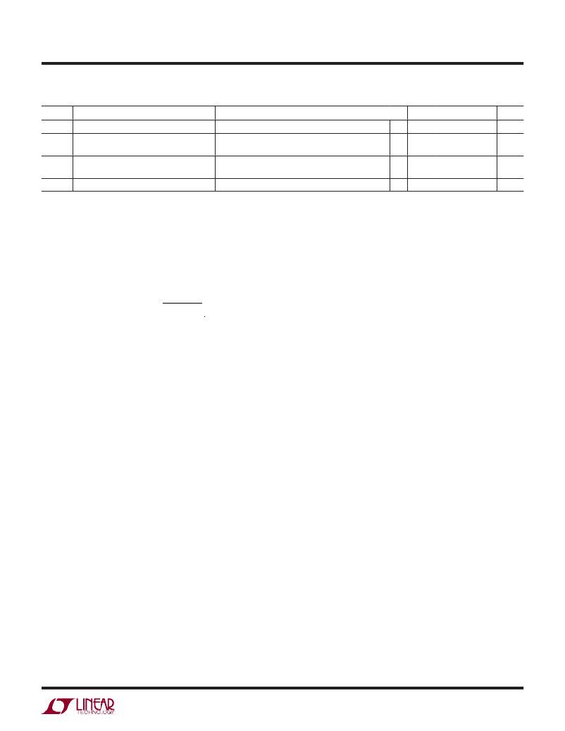
�ELECTRICAL� CHARACTERISTICS� The� l� denotes� the� specifications� which� apply� over� the� full� operating�
�temperature� range,� otherwise� specifications� are� at� T� A� =� 25°C.� V� IN� =� 15V,� V� C� =� 0.5V,� V� FB� =� V� REF� ,� output� pin� open,� unless� otherwise� noted.�
�SYMBOL� PARAMETER�
�CONDITIONS�
�MIN�
�TYP�
�MAX�
�UNITS�
�DC� MAX�
�Maximum� Switch� Duty� Cycle�
�Shutdown� Mode�
�3V� ≤� V� IN� ≤� V� MAX�
�l�
�85�
�92�
�100�
�97�
�250�
�%�
�μA�
�Supply� Current�
�V� C� =� 0.05V�
�Shutdown� Mode�
�Threshold� Voltage�
�3V� ≤� V� IN� ≤� V� MAX�
�l�
�100�
�50�
�150�
�250�
�300�
�mV�
�mV�
�Flyback� Sense� Delay� Time� (Note� 5)�
�1.5�
�μs�
�Note� 1:� Stresses� beyond� those� listed� under� Absolute� Maximum� Ratings�
�may� cause� permanent� damage� to� the� device.� Exposure� to� any� Absolute�
�Maximum� Rating� condition� for� extended� periods� may� affect� device�
�reliability� and� lifetime.�
�Note� 2:� Minimum� effective� switch� “on”� time� for� the� LT1170/LT1171/�
�LT1172� (in� current� limit� only)� is� ≈� 0.6μs.� This� limits� the� maximum� safe�
�input� voltage� during� an� output� shorted� condition.� Buck� mode� and� inverting�
�mode� input� voltage� during� an� output� shorted� condition� is� limited� to:�
�V� IN� (max,� output� shorted)� =� 15V� +� (� R� )� (� I� L� )� +� Vf�
�buck� and� inverting� mode� (� t� )� (� f� )�
�R� =� Inductor� DC� resistance�
�I� L� =� 10A� for� LT1170,� 5A� for� LT1171,� and� 2.5A� for� LT1172�
�Transformer� designs� will� tolerate� much� higher� input� voltages� because�
�leakage� inductance� limits� rate� of� rise� of� current� in� the� switch.� These�
�designs� must� be� evaluated� individually� to� assure� that� current� limit� is� well�
�controlled� up� to� maximum� input� voltage.�
�Boost� mode� designs� are� never� protected� against� output� shorts� because�
�the� external� catch� diode� and� inductor� connect� input� to� output.�
�Note� 3:� Measured� with� V� C� in� hi� clamp,� V� FB� =� 0.8V.� I� SW� =� 4A� for� LT1170,�
�2A� for� LT1171,� and� 1A� for� LT1172.�
�Note� 4:� For� duty� cycles� (DC)� between� 50%� and� 80%,� minimum� guaranteed�
�switch� current� is� given� by� I� LIM� =� 3.33� (2� –� DC)� for� the� LT1170,� I� LIM� =� 1.67�
�(2� –� DC)� for� the� LT1171,� and� I� LIM� =� 0.833� (2� –� DC)� for� the� LT1172.�
�Note� 5:� Minimum� input� voltage� for� isolated� flyback� mode� is� 7V.� V� MAX� =� 55V�
�for� HV� grade� in� fully� isolated� mode� to� avoid� switch� breakdown.�
�Vf� =� Output� catch� diode� forward� voltage� at� I� L�
�t� =� 0.6μs,� f� =� 100kHz� switching� frequency�
�Maximum� input� voltage� can� be� increased� by� increasing� R� or� Vf.�
�External� current� limiting� such� as� that� shown� in� AN19,� Figure� 39,� will�
�provide� protection� up� to� the� full� supply� voltage� rating.� C1� in� Figure� 39�
�should� be� reduced� to� 200pF.�
�117012fg�
�5�
�相关PDF资料 |
PDF描述 |
|---|---|
| 6730-RC | INDUCTOR TOROID W/HDR 70UH 15% |
| LT3688IFE#PBF | IC REG BUCK ADJ 0.8A DL 24TSSOP |
| 6729-RC | INDUCTOR TOROID W/HDR 100UH 15% |
| MIC2177-3.3YWM | IC REG BUCK SYNC 3.3V 20SOIC |
| LT3991IDD#PBF | IC REG BUCK ADJ 1.2A 10DFN |
相关代理商/技术参数 |
参数描述 |
|---|---|
| LT1171CTPBF | 制造商:Linear Technology 功能描述:LT1171CTPBF |
| LT1171HV | 制造商:LINER 制造商全称:Linear Technology 功能描述:100kHz, 5A, 2.5A and 1.25A High Efficiency Switching Regulators |
| LT1171HVC | 制造商:LINER 制造商全称:Linear Technology 功能描述:100kHz, 5A, 2.5A and 1.25A High Efficiency Switching Regulators |
| LT1171HVCQ | 功能描述:IC REG MULTI CONFIG ADJ D2PAK RoHS:否 类别:集成电路 (IC) >> PMIC - 稳压器 - DC DC 开关稳压器 系列:- 设计资源:Design Support Tool 标准包装:1 系列:- 类型:升压(升压) 输出类型:固定 输出数:1 输出电压:3V 输入电压:0.75 V ~ 2 V PWM 型:- 频率 - 开关:- 电流 - 输出:100mA 同步整流器:是 工作温度:-40°C ~ 85°C 安装类型:表面贴装 封装/外壳:SOT-23-5 细型,TSOT-23-5 包装:剪切带 (CT) 供应商设备封装:TSOT-23-5 其它名称:AS1323-BTTT-30CT |
| LT1171HVCQ#PBF | 功能描述:IC REG MULTI CONFIG ADJ D2PAK RoHS:是 类别:集成电路 (IC) >> PMIC - 稳压器 - DC DC 开关稳压器 系列:- 设计资源:Design Support Tool 标准包装:1 系列:- 类型:升压(升压) 输出类型:固定 输出数:1 输出电压:3V 输入电压:0.75 V ~ 2 V PWM 型:- 频率 - 开关:- 电流 - 输出:100mA 同步整流器:是 工作温度:-40°C ~ 85°C 安装类型:表面贴装 封装/外壳:SOT-23-5 细型,TSOT-23-5 包装:剪切带 (CT) 供应商设备封装:TSOT-23-5 其它名称:AS1323-BTTT-30CT |
发布紧急采购,3分钟左右您将得到回复。