参数资料
| 型号: | LT1187CN8 |
| 厂商: | Linear Technology |
| 文件页数: | 11/16页 |
| 文件大小: | 0K |
| 描述: | IC AMP VIDEO DIFFRNC ADJ 8-DIP |
| 标准包装: | 50 |
| 应用: | 差分 |
| 电路数: | 1 |
| -3db带宽: | 50MHz |
| 转换速率: | 165 V/µs |
| 电流 - 电源: | 13mA |
| 电流 - 输出 / 通道: | 20mA |
| 电压 - 电源,单路/双路(±): | 4.75 V ~ 16 V,±2.38 V ~ 8 V |
| 安装类型: | 通孔 |
| 封装/外壳: | 8-DIP(0.300",7.62mm) |
| 供应商设备封装: | 8-PDIP |
| 包装: | 管件 |
LT1187
4
1187fa
Note 1: Stresses beyond those listed under Absolute Maximum Ratings
may cause permanent damage to the device. Exposure to any Absolute
Maximum Rating condition for extended periods may affect device
reliability and lifetime.
Note 2: A heat sink may be required to keep the junction temperature
below absolute maximum when the output is shorted continuously.
Note 3: TJ is calculated from the ambient temperature TA and power
dissipation PD according to the following formulas:
LT1187MJ8, LT1187CJ8:
TJ = TA + (PD 100°C/W)
LT1187CN8:
TJ = TA + (PD 100°C/W)
LT1187CS8:
TJ = TA + (PD 150°C/W)
Note 4: When RL = 1k is specied, the load resistor is RFB1 + RFB2, but
when RL = 300Ω is specied, then an additional 430Ω is added to the
output such that (RFB1 + RFB2) in parallel with 430Ω is RL = 300Ω.
Note 5: VOS measured at the output (Pin 6) is the contribution from both
input pair and is input referred.
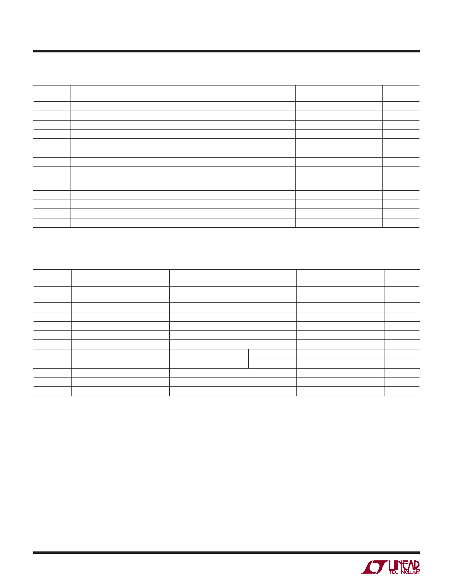
±5V ELECTRICAL CHARACTERISTICS 0°C ≤ T
A ≤ 70°C (LT1187C) –40°C ≤ TA ≤ 85°C (LT1187I) (Note 4)
VS = ±5V, VREF = 0V, RFB1 = 900Ω from Pins 6 to 8, RFB2 = 100Ω from Pin 8 to ground, RL = RFB1 + RFB2 = 1k, CL ≤ 10pF, Pin 5 open.
SYMBOL
PARAMETER
CONDITIONS
MIN
LT1187C/I
TYP
MAX
UNITS
VOS
Input Offset Voltage
Either Input (Note 5)
2.0
12
mV
ΔVOS/ΔT
Input VOS Drift
9.0
mV/°C
IOS
Input Offset Current
Either Input
0.2
1.5
A
IB
Input Bias Current
Either Input
±0.5
±3.5
A
Input Voltage Range
–2.5
3.5
V
CMRR
Common Mode Rejection Ratio
VCM = –2.5V to 3.5V
70
100
dB
PSRR
Power Supply Rejection Ratio
VS = ±2.375V to ±8V
65
85
dB
VOUT
Output Voltage Swing
VS = ±5V, RL = 1k, AV = 50
VS = ±8V, RL = 1k, AV = 50
VS = ±8V, RL = 300Ω, AV = 50 (Note 4)
±3.7
±6.6
±6.4
±4.0
±7.0
±6.8
V
GE
Gain Error
VO = ±1V, AV = 10, RL = 1k
0.2
1.0
%
IS
Supply Current
13
17
mA
Shutdown Supply Current
Pin 5 at V– (Note 12)
0.8
1.5
mA
IS/D
Shutdown Pin Current
Pin 5 at V–
525
A
5V ELECTRICAL CHARACTERISTICS 0°C ≤ T
A ≤ 70°C (LT1187C) –40°C ≤ TA ≤ 85°C (LT1187I) (Note 4)
VS
+ = 5V, VS– = 0V, VREF = 2.5V, RFB1 = 900Ω from Pins 6 to 8, RFB2 = 100Ω from Pin 8 to VREF, RL = RFB1 + RFB2 = 1k, CL ≤ 10pF, Pin 5
open.
SYMBOL
PARAMETER
CONDITIONS
MIN
LT1187C/I
TYP
MAX
UNITS
VOS
Input Offset Voltage
Either Input (Note 5)
SO Package
2.0
12.0
13.0
mV
ΔVOS/ΔT
Input VOS Drift
9.0
V/°C
IOS
Input Offset Current
Either Input
0.2
1.5
A
IB
Input Bias Current
Either Input
±0.5
±3.5
A
Input Voltage Range
2.0
3.5
V
CMRR
Common Mode Rejection Ratio
VCM = 2.0V to 3.5V
70
100
dB
VOUT
Output Voltage Swing
RL = 300Ω to Ground
(Note 4)
VOUT High
3.5
4.0
V
VOUT Low
0.15
0.4
V
IS
Supply Current
12
16
mA
Shutdown Supply Current
Pin 5 at V– (Note 12)
0.8
1.5
mA
IS/D
Shutdown Pin Current
Pin 5 at V–
525
A
Note 6: VIN LIM is the maximum voltage between –VIN and +VIN (Pin 2 and
Pin 3) for which the output can respond.
Note 7: Slew rate is measured between ±0.5V on the output, with a VIN
step of ±0.75V, AV = 3 and RL = 1k.
Note 8: Full power bandwidth is calculated from the slew rate
measurement: FPBW = SR/2
πVP.
Note 9: Settling time measurement techniques are shown in “Take the
Guesswork Out of Settling Time Measurements,” EDN, September 19,
1985.
Note 10: NTSC (3.58MHz).
Note 11: AC parameters are 100% tested on the ceramic and plastic DIP
packaged parts (J8 and N8 sufx) and are sample tested on every lot of
the SO packaged parts (S8 sufx).
Note 12: See Application section for shutdown at elevated temperatures.
Do not operate shutdown above TJ > 125°C.
相关PDF资料 |
PDF描述 |
|---|---|
| VI-JTZ-MZ-B1 | CONVERTER MOD DC/DC 2V 10W |
| VE-B3M-MU-F2 | CONVERTER MOD DC/DC 10V 200W |
| VI-JTY-MZ-B1 | CONVERTER MOD DC/DC 3.3V 16.5W |
| VE-B3L-MU-F4 | CONVERTER MOD DC/DC 28V 200W |
| VI-JTX-MZ-B1 | CONVERTER MOD DC/DC 5.2V 25W |
相关代理商/技术参数 |
参数描述 |
|---|---|
| LT1187CN8#PBF | 功能描述:IC AMP VIDEO DIFFRNC ADJ 8-DIP RoHS:是 类别:集成电路 (IC) >> 线性 - 放大器 - 视频放大器和频缓冲器 系列:- 标准包装:1,000 系列:- 应用:驱动器 输出类型:差分 电路数:3 -3db带宽:350MHz 转换速率:1000 V/µs 电流 - 电源:14.5mA 电流 - 输出 / 通道:60mA 电压 - 电源,单路/双路(±):5 V ~ 12 V,±2.5 V ~ 6 V 安装类型:表面贴装 封装/外壳:20-VFQFN 裸露焊盘 供应商设备封装:20-QFN 裸露焊盘(4x4) 包装:带卷 (TR) |
| LT1187CS8 | 功能描述:IC AMP VIDEO DIFFRNC ADJ 8-SOIC RoHS:否 类别:集成电路 (IC) >> 线性 - 放大器 - 视频放大器和频缓冲器 系列:- 标准包装:1,000 系列:- 应用:驱动器 输出类型:差分 电路数:3 -3db带宽:350MHz 转换速率:1000 V/µs 电流 - 电源:14.5mA 电流 - 输出 / 通道:60mA 电压 - 电源,单路/双路(±):5 V ~ 12 V,±2.5 V ~ 6 V 安装类型:表面贴装 封装/外壳:20-VFQFN 裸露焊盘 供应商设备封装:20-QFN 裸露焊盘(4x4) 包装:带卷 (TR) |
| LT1187CS8#PBF | 功能描述:IC AMP VIDEO DIFFRNC ADJ 8-SOIC RoHS:是 类别:集成电路 (IC) >> 线性 - 放大器 - 视频放大器和频缓冲器 系列:- 标准包装:1,000 系列:- 应用:驱动器 输出类型:差分 电路数:3 -3db带宽:350MHz 转换速率:1000 V/µs 电流 - 电源:14.5mA 电流 - 输出 / 通道:60mA 电压 - 电源,单路/双路(±):5 V ~ 12 V,±2.5 V ~ 6 V 安装类型:表面贴装 封装/外壳:20-VFQFN 裸露焊盘 供应商设备封装:20-QFN 裸露焊盘(4x4) 包装:带卷 (TR) |
| LT1187CS8#TR | 功能描述:IC AMP VID DIFF CURR FDBK 8SOIC RoHS:否 类别:集成电路 (IC) >> 线性 - 放大器 - 视频放大器和频缓冲器 系列:- 标准包装:1,000 系列:- 应用:驱动器 输出类型:差分 电路数:3 -3db带宽:350MHz 转换速率:1000 V/µs 电流 - 电源:14.5mA 电流 - 输出 / 通道:60mA 电压 - 电源,单路/双路(±):5 V ~ 12 V,±2.5 V ~ 6 V 安装类型:表面贴装 封装/外壳:20-VFQFN 裸露焊盘 供应商设备封装:20-QFN 裸露焊盘(4x4) 包装:带卷 (TR) |
| LT1187CS8#TRPBF | 功能描述:IC AMP VIDEO DIFFRNC ADJ 8-SOIC RoHS:否 类别:集成电路 (IC) >> 线性 - 放大器 - 视频放大器和频缓冲器 系列:- 标准包装:1,000 系列:- 应用:驱动器 输出类型:差分 电路数:3 -3db带宽:350MHz 转换速率:1000 V/µs 电流 - 电源:14.5mA 电流 - 输出 / 通道:60mA 电压 - 电源,单路/双路(±):5 V ~ 12 V,±2.5 V ~ 6 V 安装类型:表面贴装 封装/外壳:20-VFQFN 裸露焊盘 供应商设备封装:20-QFN 裸露焊盘(4x4) 包装:带卷 (TR) |
发布紧急采购,3分钟左右您将得到回复。