参数资料
| 型号: | LT1193CN8 |
| 厂商: | Linear Technology |
| 文件页数: | 7/12页 |
| 文件大小: | 0K |
| 描述: | IC AMP VIDEO DIF ADJ GAIN 8-DIP |
| 标准包装: | 50 |
| 应用: | 差分 |
| 电路数: | 1 |
| -3db带宽: | 80MHz |
| 转换速率: | 500 V/µs |
| 电流 - 电源: | 35mA |
| 电流 - 输出 / 通道: | 50mA |
| 电压 - 电源,单路/双路(±): | 4.75 V ~ 16 V,±2.38 V ~ 8 V |
| 安装类型: | 通孔 |
| 封装/外壳: | 8-DIP(0.300",7.62mm) |
| 供应商设备封装: | 8-PDIP |
| 包装: | 管件 |
4
LT1193
1193fb
LT1193C
SYMBOL
PARAMETER
CONDITIONS
MIN
TYP
MAX
UNITS
VOS
Input Offset Voltage
N8 Package
q
214
mV
SO-8 Package
q
20
mV
VOS/T
Input VOS Drift
q
20
V/°C
IOS
Input Offset Current
q
0.2
3.5
A
IB
Input Bias Current
q
±0.5
±4
A
Input Voltage Range
q
–2.5
3.5
V
CMRR
Common Mode Rejection Ratio
VCM = – 2.5V to 3.5V
q
55
70
dB
PSRR
Power Supply Rejection Ratio
VS = ±2.375V to ±5V
q
55
70
dB
VOUT
Output Voltage Swing
RL = 1k
q
3.7
4
V
RL = 100
q
6.2
6.6
V
GE
Gain Error
VO = ± 3V, RL = 1k
q
0.2
1.2
%
IS
Supply Current
q
35
43
mA
Shutdown Supply Current
Pin 5 at V – (Note 10)
q
1.3
2.1
mA
ISHDN
Shutdown Pin Current
Pin 5 at V –
q
20
A
Note 7: Full-power bandwidth is calculated from the slew rate
measurement:
FPBW = SR/2
πVP.
Note 8: Settling time measurement techniques are shown in “Take the
Guesswork Out of Settling Time Measurements,” EDN, September 19,
1985.
Note 9: NTSC (3.58MHz).
Note 10: See Applications section for shutdown at elevated temperatures.
Do not operate the shutdown above TJ > 125°C.
Note 11: AC parameters are 100% tested on the ceramic and plastic DIP
packaged parts (J and N suffix) and are sample tested on every lot of the
SO packaged parts (S suffix).
Note 1: Absolute Maximum Ratings are those values beyond which the
life of a device may be impaired.
Note 2: A heat sink is required to keep the junction temperature below
absolute maximum when the output is shorted.
Note 3: When RL = 1k is specified, the load resistor is RFB1 + RFB2, but
when RL = 100 is specified, then an additional 100 is added to the
output.
Note 4: VOS measured at the output (Pin 6) is the contribution from both
input pair, and is input referred.
Note 5: VIN LIM is the maximum voltage between –VIN and +VIN (Pin 2 and
Pin 3) for which the output can respond.
Note 6: Slew rate is measured between
±2V on the output, with a ±1V
input step, AV = 3.
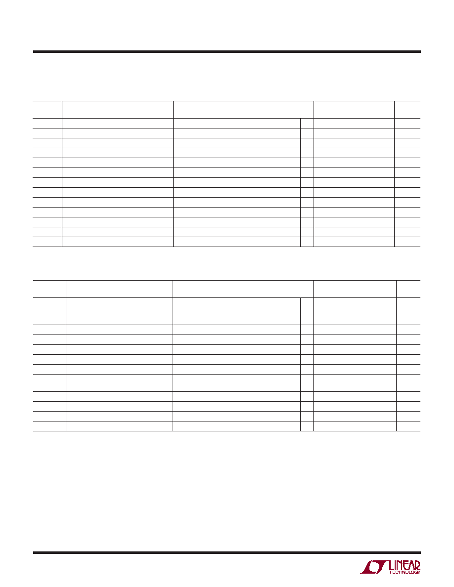
ELECTRICAL CHARACTERISTICS
The q denotes the specificatons which apply over the full operating temperature range of 0
°C ≤ TA ≤ 70°C. VS = ±5V, VREF = 0V,
RFB1 = 900 from Pins 6 to 8, RFB2 = 100 from Pin 8 to ground, RL = RFB1 + RFB2 = 1k (Note 3), CL ≤ 10pF, Pin 5 open circuit,
unless otherwise noted.
LT1193I
SYMBOL
PARAMETER
CONDITIONS
MIN
TYP
MAX
UNITS
VOS
Input Offset Voltage
SO-8 Package
q
220
mV
VOS/T Input VOS Drift
q
20
V/°C
IOS
Input Offset Current
q
0.8
5
A
IB
Input Bias Current
q
±1
±5.5
A
Input Voltage Range
q
–2.5
3.5
V
CMRR
Common Mode Rejection Ratio
VCM = – 2.5V to 3.5V
q
53
70
dB
PSRR
Power Supply Rejection Ratio
VS = ±2.375V to ±5V
q
53
70
dB
VOUT
Output Voltage Swing
RL = 1k
q
3.6
4
V
VS = ±8V, RL = 100
q
6
6.5
GE
Gain Error
VO = ±3V, RL = 1k
q
0.2
1.2
%
IS
Supply Current
q
35
43
mA
Shutdown Supply Current
Pin 5 at V – (Note 10)
q
1.3
2.2
mA
ISHDN
Shutdown Pin Current
Pin 5 at V –
q
20
A
The q denotes the specificatons which apply over the full operating temperature range of – 40
°C ≤ TA ≤ 85°C. VS = ±5V,
VREF = 0V, RFB1 = 900 from Pins 6 to 8, RFB2 = 100 from Pin 8 to ground, RL = RFB2 = 1k (Note 3), CL ≤ 10pF, Pin 5 open circuit,
unless otherwise noted.
相关PDF资料 |
PDF描述 |
|---|---|
| VE-J01-MZ-B1 | CONVERTER MOD DC/DC 12V 25W |
| LT1187CN8 | IC AMP VIDEO DIFFRNC ADJ 8-DIP |
| VI-JTZ-MZ-B1 | CONVERTER MOD DC/DC 2V 10W |
| VE-B3M-MU-F2 | CONVERTER MOD DC/DC 10V 200W |
| VI-JTY-MZ-B1 | CONVERTER MOD DC/DC 3.3V 16.5W |
相关代理商/技术参数 |
参数描述 |
|---|---|
| LT1193CN8#PBF | 功能描述:IC AMP VIDEO DIF ADJ GAIN 8-DIP RoHS:是 类别:集成电路 (IC) >> 线性 - 放大器 - 视频放大器和频缓冲器 系列:- 产品培训模块:Lead (SnPb) Finish for COTS Obsolescence Mitigation Program 标准包装:50 系列:- 应用:TFT-LCD 面板:VCOM 驱动器 输出类型:满摆幅 电路数:1 -3db带宽:35MHz 转换速率:40 V/µs 电流 - 电源:3.7mA 电流 - 输出 / 通道:1.3A 电压 - 电源,单路/双路(±):9 V ~ 20 V,±4.5 V ~ 10 V 安装类型:表面贴装 封装/外壳:8-TSSOP,8-MSOP(0.118",3.00mm 宽)裸露焊盘 供应商设备封装:8-uMax-EP 包装:管件 |
| LT1193CN8PBF | 制造商:Linear Technology 功能描述:LT1193CN8PBF |
| LT1193CS8 | 功能描述:IC AMP VIDEO DIF ADJ 8-SOIC RoHS:否 类别:集成电路 (IC) >> 线性 - 放大器 - 视频放大器和频缓冲器 系列:- 标准包装:1,000 系列:- 应用:驱动器 输出类型:差分 电路数:3 -3db带宽:350MHz 转换速率:1000 V/µs 电流 - 电源:14.5mA 电流 - 输出 / 通道:60mA 电压 - 电源,单路/双路(±):5 V ~ 12 V,±2.5 V ~ 6 V 安装类型:表面贴装 封装/外壳:20-VFQFN 裸露焊盘 供应商设备封装:20-QFN 裸露焊盘(4x4) 包装:带卷 (TR) |
| LT1193CS8#PBF | 功能描述:IC AMP VIDEO DIF ADJ 8-SOIC RoHS:是 类别:集成电路 (IC) >> 线性 - 放大器 - 视频放大器和频缓冲器 系列:- 产品培训模块:Lead (SnPb) Finish for COTS Obsolescence Mitigation Program 标准包装:50 系列:- 应用:TFT-LCD 面板:VCOM 驱动器 输出类型:满摆幅 电路数:1 -3db带宽:35MHz 转换速率:40 V/µs 电流 - 电源:3.7mA 电流 - 输出 / 通道:1.3A 电压 - 电源,单路/双路(±):9 V ~ 20 V,±4.5 V ~ 10 V 安装类型:表面贴装 封装/外壳:8-TSSOP,8-MSOP(0.118",3.00mm 宽)裸露焊盘 供应商设备封装:8-uMax-EP 包装:管件 |
| LT1193CS8#TR | 功能描述:IC AMP VIDEO DIFF ADJUST 8SOIC RoHS:否 类别:集成电路 (IC) >> 线性 - 放大器 - 视频放大器和频缓冲器 系列:- 标准包装:1,000 系列:- 应用:驱动器 输出类型:差分 电路数:3 -3db带宽:350MHz 转换速率:1000 V/µs 电流 - 电源:14.5mA 电流 - 输出 / 通道:60mA 电压 - 电源,单路/双路(±):5 V ~ 12 V,±2.5 V ~ 6 V 安装类型:表面贴装 封装/外壳:20-VFQFN 裸露焊盘 供应商设备封装:20-QFN 裸露焊盘(4x4) 包装:带卷 (TR) |
发布紧急采购,3分钟左右您将得到回复。