参数资料
| 型号: | LT1210CR#PBF |
| 厂商: | Linear Technology |
| 文件页数: | 15/16页 |
| 文件大小: | 0K |
| 描述: | IC 35MHZ 1.1 AMP AMPLIFIER 7 DD |
| 标准包装: | 50 |
| 放大器类型: | 电流反馈 |
| 电路数: | 1 |
| 转换速率: | 90 V/µs |
| -3db带宽: | 55MHz |
| 电流 - 输入偏压: | 10µA |
| 电压 - 输入偏移: | 3000µV |
| 电流 - 电源: | 35mA |
| 电流 - 输出 / 通道: | 2A |
| 电压 - 电源,单路/双路(±): | 10 V ~ 30 V,±5 V ~ 15 V |
| 工作温度: | 0°C ~ 70°C |
| 安装类型: | 表面贴装 |
| 封装/外壳: | TO-263-8,D²Pak(7 引线+接片),TO-263CA |
| 供应商设备封装: | DDPAK-7 |
| 包装: | 管件 |
8
LT1210
1210fa
U
S
A
O
PPLICATI
WU
U
I FOR ATIO
The LT1210 is a current feedback amplifier with high
output current drive capability. The device is stable with
large capacitive loads and can easily supply the high
currents required by capacitive loads. The amplifier will
drive low impedance loads such as cables with excellent
linearity at high frequencies.
Feedback Resistor Selection
The optimum value for the feedback resistors is a function
of the operating conditions of the device, the load imped-
ance and the desired flatness of response. The Typical AC
Performance tables give the values which result in less
than 1dB of peaking for various resistive loads and oper-
ating conditions. If this level of flatness is not required, a
higher bandwidth can be obtained by use of a lower
feedback resistor. The characteristic curves of Bandwidth
vs Supply Voltage indicate feedback resistors for peaking
up to 5dB. These curves use a solid line when the response
has less than 1dB of peaking and a dashed line when the
response has 1dB to 5dB of peaking. The curves stop
where the response has more than 5dB of peaking.
For resistive loads, the COMP pin should be left open (see
Capacitive Loads section).
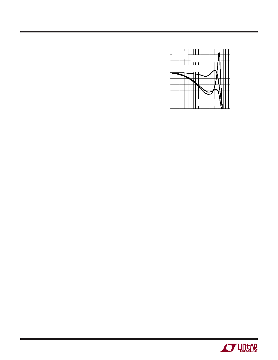
Capacitive Loads
The LT1210 includes an optional compensation network
for driving capacitive loads. This network eliminates most
of the output stage peaking associated with capacitive
loads, allowing the frequency response to be flattened.
Figure 1 shows the effect of the network on a 200pF load.
Without the optional compensation, there is a 6dB peak at
40MHz caused by the effect of the capacitance on the
output stage. Adding a 0.01
F bypass capacitor between
the output and the COMP pins connects the compensation
and greatly reduces the peaking. A lower value feedback
resistor can now be used, resulting in a response which is
flat to
±1dB to 40MHz. The network has the greatest effect
for CL in the range of 0pF to 1000pF. The graphs of
Bandwidth and Feedback Resistance vs Capacitive Load
can be used to select the appropriate value of feedback
resistor. The values shown are for 1dB and 5dB peaking at
a gain of 2 with no resistive load. This is a worst-case
condition, as the amplifier is more stable at higher gains
and with some resistive load in parallel with the capaci-
FREQUENCY (MHz)
1
–6
VOLTAGE
GAIN
(dB)
–2
2
6
10
100
1210 F01
–4
0
4
8
12
14
VS = ±15V
CL = 200pF
RF = 1.5k
COMPENSATION
RF = 3.4k
NO COMPENSATION
RF = 3.4k
COMPENSATION
Figure 1
tance. Also shown is the – 3dB bandwidth with the sug-
gested feedback resistor vs the load capacitance.
Although the optional compensation works well with
capacitive loads, it simply reduces the bandwidth when it
is connected with resistive loads. For instance, with a 10
load, the bandwidth drops from 35MHz to 26MHz when
the compensation is connected. Hence, the compensation
was made optional. To disconnect the optional compensa-
tion, leave the COMP pin open.
Shutdown/Current Set
If the shutdown feature is not used, the SHUTDOWN pin
must be connected to ground or V –.
The Shutdown pin can be used to either turn off the biasing
for the amplifier, reducing the quiescent current to less
than 200
A, or to control the quiescent current in normal
operation.
The total bias current in the LT1210 is controlled by the
current flowing out of the Shutdown pin. When the Shut-
down pin is open or driven to the positive supply, the part
is shut down. In the shutdown mode, the output looks like
a 70pF capacitor and the supply current is typically less
than 100
A. The Shutdown pin is referenced to the posi-
tive supply through an internal bias circuit (see the Simpli-
fied Schematic). An easy way to force shutdown is to use
open-drain (collector) logic. The circuit shown in Figure 2
uses a 74C904 buffer to interface between 5V logic and the
LT1210. The switching time between the active and shut-
down states is about 1
s. A 24k pull-up resistor speeds
相关PDF资料 |
PDF描述 |
|---|---|
| TSW-127-23-T-S | CONN HEADER 27POS .100" SNGL TIN |
| LT1210CT7#PBF | IC AMP C-FEEDBACK 1.1A TO-220-7 |
| TSW-118-23-L-S | CONN HEADER 18POS .100" SGL GOLD |
| AD526JNZ | IC AMP PGA 10MA 16DIP |
| TSW-102-17-G-D | CONN HEADER 4POS .100" DUAL GOLD |
相关代理商/技术参数 |
参数描述 |
|---|---|
| LT1210CS | 功能描述:IC CURRNT FEEDBK AMP 1.1A 16SOIC RoHS:否 类别:集成电路 (IC) >> Linear - Amplifiers - Instrumentation 系列:- 标准包装:150 系列:- 放大器类型:音频 电路数:2 输出类型:- 转换速率:5 V/µs 增益带宽积:12MHz -3db带宽:- 电流 - 输入偏压:100nA 电压 - 输入偏移:500µV 电流 - 电源:6mA 电流 - 输出 / 通道:50mA 电压 - 电源,单路/双路(±):4 V ~ 32 V,±2 V ~ 16 V 工作温度:-40°C ~ 85°C 安装类型:表面贴装 封装/外壳:8-TSSOP(0.173",4.40mm 宽) 供应商设备封装:8-TSSOP 包装:管件 |
| LT1210CS#PBF | 功能描述:IC CURRNT FEEDBK AMP 1.1A 16SOIC RoHS:是 类别:集成电路 (IC) >> Linear - Amplifiers - Instrumentation 系列:- 标准包装:150 系列:- 放大器类型:音频 电路数:2 输出类型:- 转换速率:5 V/µs 增益带宽积:12MHz -3db带宽:- 电流 - 输入偏压:100nA 电压 - 输入偏移:500µV 电流 - 电源:6mA 电流 - 输出 / 通道:50mA 电压 - 电源,单路/双路(±):4 V ~ 32 V,±2 V ~ 16 V 工作温度:-40°C ~ 85°C 安装类型:表面贴装 封装/外壳:8-TSSOP(0.173",4.40mm 宽) 供应商设备封装:8-TSSOP 包装:管件 |
| LT1210CS#PBF | 制造商:Linear Technology 功能描述:CURRENT FEEDBACK AMPLIFIER |
| LT1210CS#TR | 功能描述:IC AMP CURR FEEDBACK 1.1A 16SOIC RoHS:否 类别:集成电路 (IC) >> Linear - Amplifiers - Instrumentation 系列:- 标准包装:150 系列:- 放大器类型:音频 电路数:2 输出类型:- 转换速率:5 V/µs 增益带宽积:12MHz -3db带宽:- 电流 - 输入偏压:100nA 电压 - 输入偏移:500µV 电流 - 电源:6mA 电流 - 输出 / 通道:50mA 电压 - 电源,单路/双路(±):4 V ~ 32 V,±2 V ~ 16 V 工作温度:-40°C ~ 85°C 安装类型:表面贴装 封装/外壳:8-TSSOP(0.173",4.40mm 宽) 供应商设备封装:8-TSSOP 包装:管件 |
| LT1210CS#TRPBF | 功能描述:IC CURRNT FEEDBK AMP 1.1A 16SOIC RoHS:是 类别:集成电路 (IC) >> Linear - Amplifiers - Instrumentation 系列:- 标准包装:150 系列:- 放大器类型:音频 电路数:2 输出类型:- 转换速率:5 V/µs 增益带宽积:12MHz -3db带宽:- 电流 - 输入偏压:100nA 电压 - 输入偏移:500µV 电流 - 电源:6mA 电流 - 输出 / 通道:50mA 电压 - 电源,单路/双路(±):4 V ~ 32 V,±2 V ~ 16 V 工作温度:-40°C ~ 85°C 安装类型:表面贴装 封装/外壳:8-TSSOP(0.173",4.40mm 宽) 供应商设备封装:8-TSSOP 包装:管件 |
发布紧急采购,3分钟左右您将得到回复。