参数资料
| 型号: | LT1210CT7#PBF |
| 厂商: | Linear Technology |
| 文件页数: | 2/16页 |
| 文件大小: | 0K |
| 描述: | IC AMP C-FEEDBACK 1.1A TO-220-7 |
| 标准包装: | 50 |
| 放大器类型: | 电流反馈 |
| 电路数: | 1 |
| 转换速率: | 90 V/µs |
| -3db带宽: | 55MHz |
| 电流 - 输入偏压: | 10µA |
| 电压 - 输入偏移: | 3000µV |
| 电流 - 电源: | 35mA |
| 电流 - 输出 / 通道: | 2A |
| 电压 - 电源,单路/双路(±): | 10 V ~ 30 V,±5 V ~ 15 V |
| 工作温度: | 0°C ~ 70°C |
| 安装类型: | 通孔 |
| 封装/外壳: | TO-220-7 成形引线 |
| 供应商设备封装: | TO-220-7 |
| 包装: | 管件 |
| 产品目录页面: | 1317 (CN2011-ZH PDF) |
10
LT1210
1210fa
U
S
A
O
PPLICATI
WU
U
I FOR ATIO
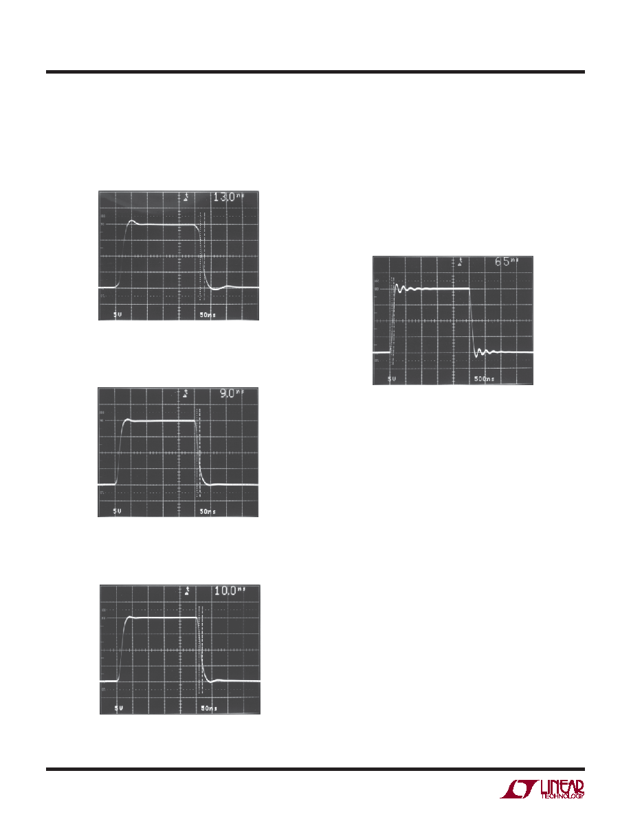
When the LT1210 is used to drive capacitive loads, the
available output current can limit the overall slew rate. In
the fastest configuration, the LT1210 is capable of a slew
rate of over 1V/ns. The current required to slew a capacitor
at this rate is 1mA per picofarad of capacitance, so
10,000pF would require 10A! The photo (Figure 6) shows
the large-signal behavior with CL = 10,000pF. The slew
rate is about 150V/
s, determined by the current limit of
1.5A.
the bandwidth is reduced. The photos in Figures 5a, 5b and
5c show the large-signal response of the LT1210 for
various gain configurations. The slew rate varies from
770V/
s for a gain of 1, to 1100V/s for a gain of –1.
1210 F05c
RF = RG = 750
RL = 10
Figure 5c. Large-Signal Response, AV = 2
Figure 5a. Large-Signal Response, AV = 1
1210 F05a
RF = 825
RL = 10
VS = ±15V
RF = RG = 750
RL = 10
VS = ±15V
1210 F05b
1210 F06
RF = RG = 3k
RL =
∞
VS = ±15V
Differential Input Signal Swing
The differential input swing is limited to about
±6V by an
ESD protection device connected between the inputs. In
normal operation, the differential voltage between the
input pins is small, so this clamp has no effect; however,
in the shutdown mode the differential swing can be the
same as the input swing. The clamp voltage will then set
the maximum allowable input voltage. To allow for some
margin, it is recommended that the input signal be less
than
±5V when the device is shut down.
Capacitance on the Inverting Input
Current feedback amplifiers require resistive feedback
from the output to the inverting input for stable operation.
Take care to minimize the stray capacitance between the
output and the inverting input. Capacitance on the invert-
ing input to ground will cause peaking in the frequency
response (and overshoot in the transient response), but it
does not degrade the stability of the amplifier.
Figure 5b. Large-Signal Response, AV = –1
Figure 6. Large-Signal Response, CL = 10,000pF
VS = ±15V
相关PDF资料 |
PDF描述 |
|---|---|
| TSW-118-23-L-S | CONN HEADER 18POS .100" SGL GOLD |
| AD526JNZ | IC AMP PGA 10MA 16DIP |
| TSW-102-17-G-D | CONN HEADER 4POS .100" DUAL GOLD |
| TSW-130-07-T-S | CONN HEADER 30POS .100" SNGL TIN |
| TSW-116-07-L-S | CONN HEADER 16POS .100" SGL GOLD |
相关代理商/技术参数 |
参数描述 |
|---|---|
| LT1211 | 制造商:LINER 制造商全称:Linear Technology 功能描述:14MHz, 7V/us, Single Supply Dual and Quad Precision Op Amps |
| LT1211ACN8 | 功能描述:IC PREC OP-AMP 14MHZ DUAL 8-DIP RoHS:否 类别:集成电路 (IC) >> Linear - Amplifiers - Instrumentation 系列:- 标准包装:50 系列:- 放大器类型:J-FET 电路数:2 输出类型:- 转换速率:3.5 V/µs 增益带宽积:1MHz -3db带宽:- 电流 - 输入偏压:30pA 电压 - 输入偏移:2000µV 电流 - 电源:200µA 电流 - 输出 / 通道:- 电压 - 电源,单路/双路(±):7 V ~ 36 V,±3.5 V ~ 18 V 工作温度:0°C ~ 70°C 安装类型:通孔 封装/外壳:8-DIP(0.300",7.62mm) 供应商设备封装:8-PDIP 包装:管件 |
| LT1211ACN8#PBF | 功能描述:IC PREC OP-AMP 14MHZ DUAL 8-DIP RoHS:是 类别:集成电路 (IC) >> Linear - Amplifiers - Instrumentation 系列:- 标准包装:50 系列:- 放大器类型:J-FET 电路数:2 输出类型:- 转换速率:3.5 V/µs 增益带宽积:1MHz -3db带宽:- 电流 - 输入偏压:30pA 电压 - 输入偏移:2000µV 电流 - 电源:200µA 电流 - 输出 / 通道:- 电压 - 电源,单路/双路(±):7 V ~ 36 V,±3.5 V ~ 18 V 工作温度:0°C ~ 70°C 安装类型:通孔 封装/外壳:8-DIP(0.300",7.62mm) 供应商设备封装:8-PDIP 包装:管件 |
| LT1211AMJ8 | 制造商:Linear Technology 功能描述:OP Amp Dual GP ±18V/36V 8-Pin CDIP 制造商:Linear Technology 功能描述:OP Amp Dual GP 18V/36V 8-Pin CDIP |
| LT1211C | 制造商:LINER 制造商全称:Linear Technology 功能描述:14MHz, 7V/us, Single Supply Dual and Quad Precision Op Amps |
发布紧急采购,3分钟左右您将得到回复。