- 您现在的位置:买卖IC网 > PDF目录10080 > LT1237CSW#PBF (Linear Technology)IC TXRX 5V RS232 ADV LOPWR28SOIC PDF资料下载
参数资料
| 型号: | LT1237CSW#PBF |
| 厂商: | Linear Technology |
| 文件页数: | 5/8页 |
| 文件大小: | 0K |
| 描述: | IC TXRX 5V RS232 ADV LOPWR28SOIC |
| 标准包装: | 27 |
| 类型: | 收发器 |
| 驱动器/接收器数: | 3/5 |
| 规程: | RS232 |
| 电源电压: | 4.5 V ~ 5.5 V |
| 安装类型: | 表面贴装 |
| 封装/外壳: | 28-SOIC(0.295",7.50mm 宽) |
| 供应商设备封装: | 28-SOIC |
| 包装: | 管件 |
5
LT1237
CC
HARA TERISTICS
UW
A
TYPICALPERFOR
CE
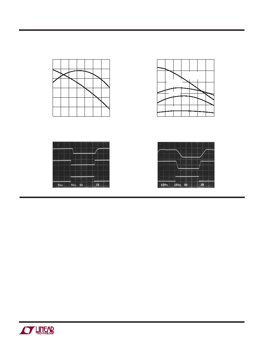
Receiver Short-Circuit Current
Driver Short-Circuit Current
TEMPERATURE (
°C)
–55
SHORT-CIRCUIT
CURRENT
(mA)
20
25
30
25
75
1237 G10
15
10
–25
0
50
100
125
5
0
ISC
+
ISC
–
TEMPERATURE (
°C)
–55
0
SHORT-CIRCUIT
CURRENT
(mA)
20
50
0
50
75
1237 G11
10
40
30
–25
25
100
125
RX1 TO RX4
ISC
+
RX1 TO RX4
ISC
–
RX5 ISC
–
RX5 ISC
+
Receiver Output Waveforms
DRIVER OUTPUT
RL = 3k
DRIVER OUTPUT
RL = 3k
CL = 2500pF
RX5 OUTPUT
CL = 50pF
1237 G12
RX1 TO RX4
OUTPUT
CL = 50pF
INPUT
1237 G13
INPUT
Driver Output Waveforms
PI FU CTIO S
U
UU
VCC: 5V Input Supply Pin. This pin should be decoupled
with a 0.1
F ceramic capacitor close to the package pin.
Insufficient supply bypassing can result in low output
drive levels and erratic charge pump operation.
GND: Ground Pin.
ON/OFF: TTL/CMOS Compatible Operating Mode Control.
A logic low puts the device in the low power shutdown
mode. All three drivers and four receivers (RX1, RX2, RX3,
and RX4) assume a high impedance output state in shut-
down. Only receiver RX5 remains active while the trans-
ceiver is in shutdown. The transceiver consumes only
60
A of supply current while in shutdown. A logic high
fully enables the transceiver.
DRIVER DISABLE: This pin provides an alternate control
for the charge pump and RS232 drivers. A logic high on
this pin shuts down the charge pump and places all driver
outputs in a high impedance state. All five receivers remain
active under these conditions. Floating the driver disable
pin or driving it to a logic low level fully enables the
transceiver. A logic low on the ON/OFF pin supersedes the
state of the DRIVER DISABLE pin. Supply current drops to
3mA when in driver disable mode.
V+: Positive Supply Output (RS232 Drivers). V+
≈ 2VCC –
1.5V. This pin requires an external charge storage capaci-
tor C
≥ 1.0F, tied to ground or VCC. Larger value capaci-
tors may be used to reduce supply ripple. The ratio of the
capacitors on V+ and V – should be greater than 5 to 1.
V–: Negative Supply Output (RS232 Drivers). V –
≈
–(2VCC – 2.5V). This pin requires an external charge
storage capacitor C
≥ 0.1F. See the Applications Infor-
mation section for guidance in choosing filter capacitors
for V+ and V –.
相关PDF资料 |
PDF描述 |
|---|---|
| MS27472T10F99S | CONN RCPT 7POS WALL MT W/SCKT |
| VI-24W-MX-F3 | CONVERTER MOD DC/DC 5.5V 75W |
| LT1237CSW | IC TXRX 5V RS232 ADV LOPWR28SOIC |
| LT1237CNW | IC TXRX 5V RS232 ADV LOPWR 28DIP |
| LTC1750CFW | IC ADC 14BIT 80MSPS SMPL 48TSSOP |
相关代理商/技术参数 |
参数描述 |
|---|---|
| LT1237IJ | 制造商:未知厂家 制造商全称:未知厂家 功能描述:Transceiver |
| LT1237IN | 制造商:未知厂家 制造商全称:未知厂家 功能描述:Transceiver |
| LT1239 | 制造商:LINER 制造商全称:Linear Technology 功能描述:Backup Battery Management Circuit |
| LT1239_02 | 制造商:LINER 制造商全称:Linear Technology 功能描述:Backup Battery Management Circuit |
| LT1239CS | 功能描述:IC BATT BACKUP MNGMNT SYS 16SOIC RoHS:否 类别:集成电路 (IC) >> PMIC - 电池管理 系列:- 标准包装:1 系列:- 功能:充电管理 电池化学:锂离子(Li-Ion)、锂聚合物(Li-Pol) 电源电压:3.75 V ~ 6 V 工作温度:-40°C ~ 85°C 安装类型:表面贴装 封装/外壳:SC-74A,SOT-753 供应商设备封装:SOT-23-5 包装:剪切带 (CT) 产品目录页面:669 (CN2011-ZH PDF) 其它名称:MCP73831T-2ACI/OTCT |
发布紧急采购,3分钟左右您将得到回复。