参数资料
| 型号: | LT1251CS#PBF |
| 厂商: | Linear Technology |
| 文件页数: | 6/24页 |
| 文件大小: | 0K |
| 描述: | IC AMP VIDEO FADE CONTRLD 14SOIC |
| 标准包装: | 55 |
| 应用: | 电流反馈 |
| 电路数: | 1 |
| -3db带宽: | 40MHz |
| 转换速率: | 300 V/µs |
| 电流 - 电源: | 14.5mA |
| 电流 - 输出 / 通道: | 40mA |
| 电压 - 电源,单路/双路(±): | 5 V ~ 30 V,±2.5 V ~ 15 V |
| 安装类型: | 表面贴装 |
| 封装/外壳: | 14-SOIC(0.154",3.90mm 宽) |
| 供应商设备封装: | 14-SOIC |
| 包装: | 管件 |
14
LT1251/LT1256
APPLICATIONS INFORMATION
WU
U
Control Circuit Description
1251/56 F03
IFS
IC
VC
VFS
IFS
RFS
V+
RC
3
5
12
11
10
4
–
+
–
+
CONTROL V TO I
FULL SCALE V TO I
CFS
RFS
5k
RC
5k
gain) is
±3% as detailed in the electrical tables. By using
a 2.5V full-scale voltage and the internal resistors, no
additional errors need be accounted for.
In the LT1256, K changes linearly with IC. To insure that K
is zero, VC must be negative 15mV or more to overcome
the worst-case control op amp offset. Similarly to insure
that K is 100%, VC must be 3% larger than VFS based on
the guaranteed gain accuracy.
To eliminate the overdrive requirement, the LT1251 has
internal circuitry that senses when the control current is at
about 5% and sets K to 0%. Similarly, at about 95% it sets
K to 100%. The LT1251 guarantees that a 2% (50mV)
input gives zero and 98% (2.45V) gives 100%.
The operating currents of the LT1251/LT1256 are derived
from IFS and therefore the quiescent current is a function
of VFS and RFS. The electrical tables show the supply
current for three values of VFS including zero. An approxi-
mate formula for the supply current is:
IS = 1mA + (24)(IFS) + (VS/20k)
where VS is the total supply voltage between Pins 9 and 7.
By reducing IFS the supply current can be reduced, how-
ever, the slew rate and bandwidth will also be reduced as
indicated in the characteristic curves. Using the internal
resistors (5k) with VFS equal to 2.5V results in IFS equal to
500
A; there is no reason to use a larger value of IFS.
The inverting inputs of the V-to-I converters are available
so that external resistors can be used instead of the
internal ones. For example, if a 10V full-scale voltage is
desired, an external pair of 20k resistors should be used to
set IFS to 500A. The positive supply voltage must be 2.5V
greater than the maximum VC and/or VFS to keep the
transistors from saturating. Do not use the internal resis-
tors with external resistors because the internal resistors
have a large positive temperature coefficient (0.2%/
°C)
that will cause gain errors.
If the control voltage is applied to the free end of resistor
RC (Pin 5) and the VC input (Pin 3) is grounded, the polarity
of the control voltage must be inverted. Therefore, K will
be 0% for zero input and 100% for – 2.5V input, assuming
VFS equals 2.5V. With Pin 3 grounded, Pin 4 is a virtual
ground; this is convenient for summing several negative
going control signals.
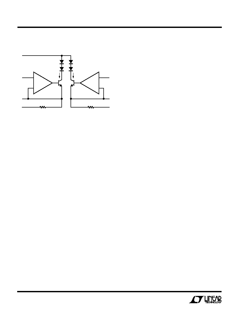
The control section of the LT1251/LT1256 consists of two
identical voltage-to-current converters (V-to-I); each
V-to-I contains an op amp, an NPN transistor and a
resistor. The converter on the right generates a
full-scale
current IFS and the one on the left generates a control
current IC. The ratio IC/IFS is called K. K goes from a
minimum of zero (when IC is zero) to a maximum of one
(when IC is equal to, or greater than, IFS). K determines the
gain from each signal input to the output.
The op amp in each V-to-I drives the transistor until the
voltage at the inverting input is the same as the voltage at
the noninverting input. If the open end of the resistor (Pin
5 or 10) is grounded, the voltage across the resistor is the
same as the voltage at the noninverting input. The emitter
current is therefore equal to the input voltage VC divided by
the resistor value RC. The collector current is essentially
the same as the emitter current and it is the ratio of the two
collector currents that sets the gain.
The LT1251/LT1256 are tested with Pins 5 and 10 grounded
and a full-scale voltage of 2.5V applied to VFS (Pin 12). This
sets IFS at approximately 500A; the control voltage VC is
applied to Pin 3. When the control voltage is negative or
zero, IC is zero and K is zero. When VC is 2.5V or greater,
IC is equal to or greater than IFS and K is one. The gain of
channel one goes from 0% to 100% as VC goes from zero
to 2.5V. The gain of channel two goes the opposite way,
from 100% down to 0%. The worst-case error in K (the
Figure 3. Control Circuit Block Diagram
相关PDF资料 |
PDF描述 |
|---|---|
| VE-BN3-MU-F1 | CONVERTER MOD DC/DC 24V 200W |
| VE-BN2-MU-F4 | CONVERTER MOD DC/DC 15V 200W |
| VE-BN2-MU-F3 | CONVERTER MOD DC/DC 15V 200W |
| AD8013AR-14 | IC OPAMP SINGLE SUPPLY 14-SOIC |
| LT1256CS | IC AMP VIDEO FADE CONTRLD 14SOIC |
相关代理商/技术参数 |
参数描述 |
|---|---|
| LT1252 | 制造商:LINER 制造商全称:Linear Technology 功能描述:Low Cost Video Amplifier |
| LT1252CN8 | 功能描述:IC AMP VIDEO LOW COST SNGL 8-DIP RoHS:否 类别:集成电路 (IC) >> 线性 - 放大器 - 视频放大器和频缓冲器 系列:- 标准包装:1,000 系列:- 应用:驱动器 输出类型:差分 电路数:3 -3db带宽:350MHz 转换速率:1000 V/µs 电流 - 电源:14.5mA 电流 - 输出 / 通道:60mA 电压 - 电源,单路/双路(±):5 V ~ 12 V,±2.5 V ~ 6 V 安装类型:表面贴装 封装/外壳:20-VFQFN 裸露焊盘 供应商设备封装:20-QFN 裸露焊盘(4x4) 包装:带卷 (TR) |
| LT1252CN8#PBF | 功能描述:IC AMP VIDEO LOW COST SNGL 8-DIP RoHS:是 类别:集成电路 (IC) >> 线性 - 放大器 - 视频放大器和频缓冲器 系列:- 产品培训模块:Lead (SnPb) Finish for COTS Obsolescence Mitigation Program 标准包装:50 系列:- 应用:TFT-LCD 面板:VCOM 驱动器 输出类型:满摆幅 电路数:1 -3db带宽:35MHz 转换速率:40 V/µs 电流 - 电源:3.7mA 电流 - 输出 / 通道:1.3A 电压 - 电源,单路/双路(±):9 V ~ 20 V,±4.5 V ~ 10 V 安装类型:表面贴装 封装/外壳:8-TSSOP,8-MSOP(0.118",3.00mm 宽)裸露焊盘 供应商设备封装:8-uMax-EP 包装:管件 |
| LT1252CS8 | 功能描述:IC AMP VIDEO LOW COST SNGL 8SOIC RoHS:否 类别:集成电路 (IC) >> 线性 - 放大器 - 视频放大器和频缓冲器 系列:- 标准包装:1,000 系列:- 应用:驱动器 输出类型:差分 电路数:3 -3db带宽:350MHz 转换速率:1000 V/µs 电流 - 电源:14.5mA 电流 - 输出 / 通道:60mA 电压 - 电源,单路/双路(±):5 V ~ 12 V,±2.5 V ~ 6 V 安装类型:表面贴装 封装/外壳:20-VFQFN 裸露焊盘 供应商设备封装:20-QFN 裸露焊盘(4x4) 包装:带卷 (TR) |
| LT1252CS8#PBF | 功能描述:IC AMP VIDEO LOW COST SNGL 8SOIC RoHS:是 类别:集成电路 (IC) >> 线性 - 放大器 - 视频放大器和频缓冲器 系列:- 产品培训模块:Lead (SnPb) Finish for COTS Obsolescence Mitigation Program 标准包装:50 系列:- 应用:TFT-LCD 面板:VCOM 驱动器 输出类型:满摆幅 电路数:1 -3db带宽:35MHz 转换速率:40 V/µs 电流 - 电源:3.7mA 电流 - 输出 / 通道:1.3A 电压 - 电源,单路/双路(±):9 V ~ 20 V,±4.5 V ~ 10 V 安装类型:表面贴装 封装/外壳:8-TSSOP,8-MSOP(0.118",3.00mm 宽)裸露焊盘 供应商设备封装:8-uMax-EP 包装:管件 |
发布紧急采购,3分钟左右您将得到回复。