- 您现在的位置:买卖IC网 > PDF目录14134 > LT1307BCS8#TR (Linear Technology)IC REG BOOST 3.3V/5V 0.1A 8SOIC PDF资料下载
参数资料
| 型号: | LT1307BCS8#TR |
| 厂商: | Linear Technology |
| 文件页数: | 8/20页 |
| 文件大小: | 0K |
| 描述: | IC REG BOOST 3.3V/5V 0.1A 8SOIC |
| 标准包装: | 2,500 |
| 类型: | 升压(升压) |
| 输出类型: | 固定 |
| 输出数: | 1 |
| 输出电压: | 3.3V,5V |
| 输入电压: | 1 V ~ 5 V |
| PWM 型: | 电流模式,混合 |
| 频率 - 开关: | 600kHz |
| 电流 - 输出: | 100mA |
| 同步整流器: | 无 |
| 工作温度: | -40°C ~ 85°C |
| 安装类型: | 表面贴装 |
| 封装/外壳: | 8-SOIC(0.154",3.90mm 宽) |
| 包装: | 带卷 (TR) |
| 供应商设备封装: | 8-SOIC |
�� �
�
�LT1307/LT1307B�
�APPLICATIO� S� I� FOR� ATIO�
�TRACE� A� 500mV/DIV�
�OPERATION�
�The� LT1307� combines� a� current� mode,� fixed� frequency�
�PWM� architecture� with� Burst� Mode� micropower� operation�
�to� maintain� high� efficiency� at� light� loads.� Operation� can�
�best� be� understood� by� referring� to� the� block� diagram� in�
�Figure� 2.� Q1� and� Q2� form� a� bandgap� reference� core� whose�
�loop� is� closed� around� the� output� of� the� converter.� When�
�V� IN� is� 1V,� the� feedback� voltage� of� 1.22V,� along� with� an�
�80mV� drop� across� R5� and� R6,� forward� biases� Q1� and� Q2’s�
�base� collector� junctions� to� 300mV.� Because� this� is� not�
�enough� to� saturate� either� transistor,� FB� can� be� at� a� higher�
�voltage� than� V� IN� .� When� there� is� no� load,� FB� rises� slightly�
�above� 1.22V,� causing� V� C� (the� error� amplifier’s� output)� to�
�decrease.� When� V� C� reaches� the� bias� voltage� on� hysteretic�
�comparator� A1,� A1’s� output� goes� low,� turning� off� all�
�circuitry� except� the� input� stage,� error� amplifier� and� low-�
�battery� detector.� Total� current� consumption� in� this� state� is�
�50� μ� A.� As� output� loading� causes� the� FB� voltage� to� de-�
�crease,� A1’s� output� goes� high,� enabling� the� rest� of� the� IC.�
�Switch� current� is� limited� to� approximately� 100mA� initially�
�after� A1’s� output� goes� high.� If� the� load� is� light,� the� output�
�voltage� (and� FB� voltage)� will� increase� until� A1’s� output�
�goes� low,� turning� off� the� rest� of� the� LT1307.� Low� fre-�
�quency� ripple� voltage� appears� at� the� output.� The� ripple�
�200mV.� There� is� no� hysteresis� in� A4,� allowing� it� to� be� used�
�as� an� amplifier� in� some� applications.� The� entire� device� is�
�disabled� when� the� SHDN� pin� is� brought� low.� To� enable� the�
�converter,� SHDN� must� be� at� V� IN� or� at� a� higher� voltage.�
�The� LT1307B� differs� from� the� LT1307� in� that� there� is� no�
�hysteresis� in� comparator� A1.� Also,� the� bias� point� on� A1� is�
�set� lower� than� on� the� LT1307� so� that� switching� can� occur�
�at� inductor� current� less� than� 100mA.� Because� A1� has� no�
�hysteresis,� there� is� no� Burst� Mode� operation� at� light� loads�
�and� the� device� continues� switching� at� constant� frequency.�
�This� results� in� the� absence� of� low� frequency� output� voltage�
�ripple� at� the� expense� of� efficiency.�
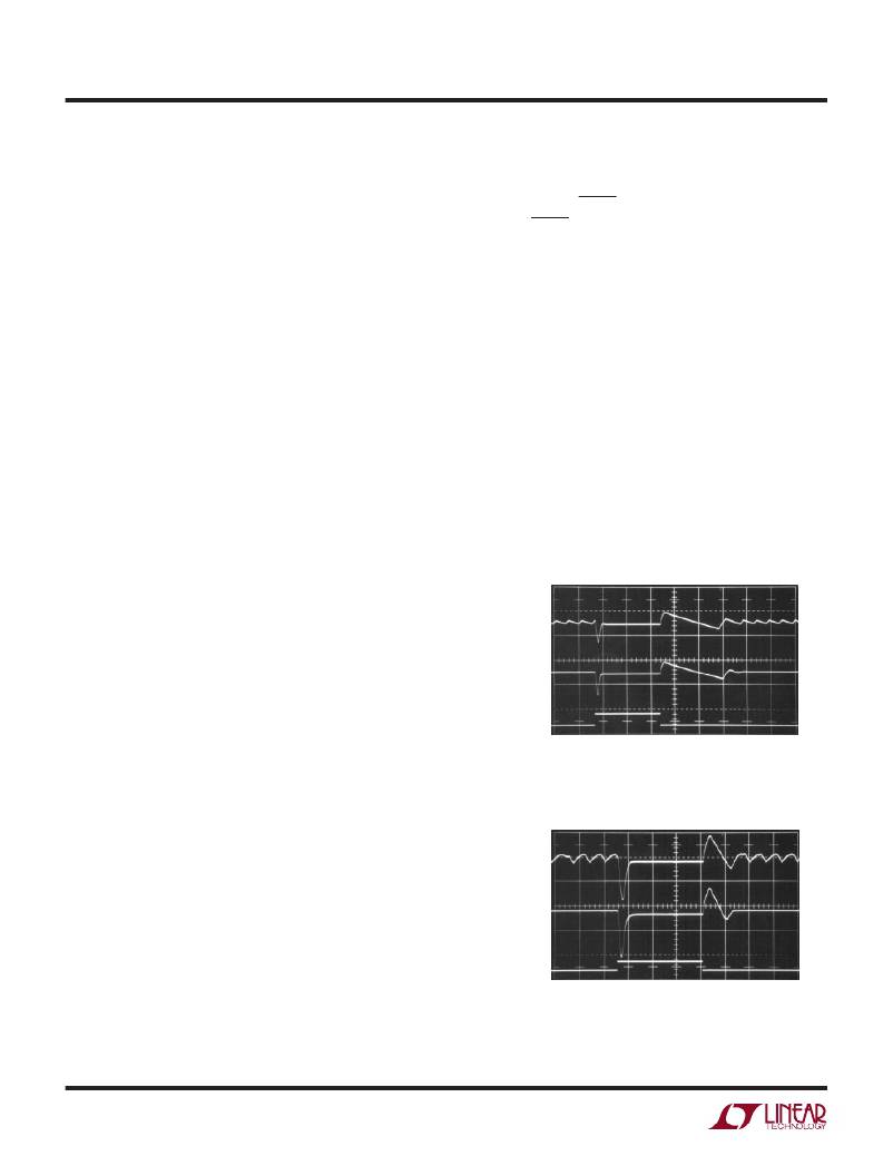
�The� difference� between� the� two� devices� is� clearly� illus-�
�trated� in� Figures� 3� and� 4.� The� top� two� traces� in� Figure� 3�
�show� an� LT1307/LT1307B� circuit,� using� the� components�
�indicated� in� Figure� 1,� set� to� a� 5V� output.� Input� voltage� is�
�1.25V.� Load� current� is� stepped� from� 1mA� to� 41mA� for� both�
�circuits.� Low� frequency� Burst� Mode� operation� voltage�
�ripple� is� observed� on� Trace� A,� while� none� is� observed� on�
�LT1307�
�V� OUT�
�AC� COUPLED�
�I� L� 41mA�
�frequencyisdependentonloadcurrentandoutputcapaci-�
�tance.� This� Burst� Mode� operation� keeps� the� output� regu-�
�lated� and� reduces� average� current� into� the� IC,� resulting� in�
�high� efficiency� even� at� load� currents� of� 100� μ� A� or� less.�
�TRACE� B�
�LT1307B�
�V� OUT�
�500mV/DIV�
�AC� COUPLED�
�1mA�
�If� the� output� load� increases� sufficiently,� A1’s� output� re-�
�V� IN� =� 1.25V�
�V� OUT� =� 5V�
�1ms/DIV�
�1307� F03�
�TRACE� A� 200mV/DIV�
�mains high, resulting in continuous operation. When the�
�LT1307� is� running� continuously,� peak� switch� current� is�
�controlled� by� V� C� to� regulate� the� output� voltage.� The� switch�
�is� turned� on� at� the� beginning� of� each� switch� cycle.� When�
�the� summation� of� a� signal� representing� switch� current� and�
�a� ramp� generator� (introduced� to� avoid� subharmonic� oscil-�
�Figure� 3.� LT1307� Exhibits� Burst� Mode� Operation� Ripple� at�
�1mA� Load,� LT1307B� Does� Not�
�LT1307�
�V� OUT�
�AC� COUPLED�
�lations� at� duty� factors� greater� than� 50%)� exceeds� the� V� C�
�signal,� comparator� A2� changes� state,� resetting� the� flip-�
�flop� and� turning� off� the� switch.� Output� voltage� increases� as�
�TRACE� B�
�LT1307B�
�V� OUT�
�200mV/DIV�
�AC� COUPLED�
�I� L� 45mA�
�switch current is increased. The output, attenuated by a�
�resistor� divider,� appears� at� the� FB� pin,� closing� the� overall�
�loop.� Frequency� compensation� is� provided� by� an� external�
�5mA�
�V� IN� =� 1.5V�
�V� OUT� =� 5V�
�500� μ� s/DIV�
�1307� F04�
�series� RC� network� connected� between� the� V� C� pin� and�
�ground.� Low-battery� detector� A4’s� open� collector� output�
�(LBO)� pulls� low� when� the� LBI� pin� voltage� drops� below�
�Figure� 4.� At� Higher� Loading� and� a� 1.5V� Supply,� LT1307�
�Again� Exhibits� Burst� Mode� Operation� Ripple� at� 5mA� Load,�
�LT1307B� Does� Not�
�1307fa�
�8�
�相关PDF资料 |
PDF描述 |
|---|---|
| MAX6867UK17D4L+T | IC MPU SUPERVISOR SOT23-5 |
| VE-J5L-CZ-F3 | CONVERTER MOD DC/DC 28V 25W |
| LNY2V103MSEG | CAP ALUM 10000UF 350V 20% SCREW |
| VE-J5L-CZ-F2 | CONVERTER MOD DC/DC 28V 25W |
| VE-J53-CZ-F4 | CONVERTER MOD DC/DC 24V 25W |
相关代理商/技术参数 |
参数描述 |
|---|---|
| LT1307BIS8 | 功能描述:IC REG BOOST 3.3V/5V 0.1A 8SOIC RoHS:否 类别:集成电路 (IC) >> PMIC - 稳压器 - DC DC 开关稳压器 系列:- 标准包装:2,500 系列:- 类型:升压(升压) 输出类型:可调式 输出数:1 输出电压:1.24 V ~ 30 V 输入电压:1.5 V ~ 12 V PWM 型:电流模式,混合 频率 - 开关:600kHz 电流 - 输出:500mA 同步整流器:无 工作温度:-40°C ~ 85°C 安装类型:表面贴装 封装/外壳:8-SOIC(0.154",3.90mm 宽) 包装:带卷 (TR) 供应商设备封装:8-SOIC |
| LT1307BIS8#PBF | 功能描述:IC REG BOOST 3.3V/5V 0.1A 8SOIC RoHS:是 类别:集成电路 (IC) >> PMIC - 稳压器 - DC DC 开关稳压器 系列:- 标准包装:2,500 系列:- 类型:升压(升压) 输出类型:可调式 输出数:1 输出电压:1.24 V ~ 30 V 输入电压:1.5 V ~ 12 V PWM 型:电流模式,混合 频率 - 开关:600kHz 电流 - 输出:500mA 同步整流器:无 工作温度:-40°C ~ 85°C 安装类型:表面贴装 封装/外壳:8-SOIC(0.154",3.90mm 宽) 包装:带卷 (TR) 供应商设备封装:8-SOIC |
| LT1307BIS8#TR | 功能描述:IC REG BOOST 3.3V/5V 0.1A 8SOIC RoHS:否 类别:集成电路 (IC) >> PMIC - 稳压器 - DC DC 开关稳压器 系列:- 标准包装:2,500 系列:- 类型:升压(升压) 输出类型:可调式 输出数:1 输出电压:1.24 V ~ 30 V 输入电压:1.5 V ~ 12 V PWM 型:电流模式,混合 频率 - 开关:600kHz 电流 - 输出:500mA 同步整流器:无 工作温度:-40°C ~ 85°C 安装类型:表面贴装 封装/外壳:8-SOIC(0.154",3.90mm 宽) 包装:带卷 (TR) 供应商设备封装:8-SOIC |
| LT1307BIS8#TRPBF | 功能描述:IC REG BOOST 3.3V/5V 0.1A 8SOIC RoHS:是 类别:集成电路 (IC) >> PMIC - 稳压器 - DC DC 开关稳压器 系列:- 标准包装:2,500 系列:- 类型:升压(升压) 输出类型:可调式 输出数:1 输出电压:1.24 V ~ 30 V 输入电压:1.5 V ~ 12 V PWM 型:电流模式,混合 频率 - 开关:600kHz 电流 - 输出:500mA 同步整流器:无 工作温度:-40°C ~ 85°C 安装类型:表面贴装 封装/外壳:8-SOIC(0.154",3.90mm 宽) 包装:带卷 (TR) 供应商设备封装:8-SOIC |
| LT1307CMS8 | 功能描述:IC REG BOOST 3.3V/5V 0.1A 8MSOP RoHS:否 类别:集成电路 (IC) >> PMIC - 稳压器 - DC DC 开关稳压器 系列:- 标准包装:2,500 系列:- 类型:升压(升压) 输出类型:可调式 输出数:1 输出电压:1.24 V ~ 30 V 输入电压:1.5 V ~ 12 V PWM 型:电流模式,混合 频率 - 开关:600kHz 电流 - 输出:500mA 同步整流器:无 工作温度:-40°C ~ 85°C 安装类型:表面贴装 封装/外壳:8-SOIC(0.154",3.90mm 宽) 包装:带卷 (TR) 供应商设备封装:8-SOIC |
发布紧急采购,3分钟左右您将得到回复。