- 您现在的位置:买卖IC网 > PDF目录14788 > LT1370CR#PBF (Linear Technology)IC REG MULTI CONFIG ADJ 6A D2PAK PDF资料下载
参数资料
| 型号: | LT1370CR#PBF |
| 厂商: | Linear Technology |
| 文件页数: | 5/16页 |
| 文件大小: | 0K |
| 描述: | IC REG MULTI CONFIG ADJ 6A D2PAK |
| 标准包装: | 50 |
| 类型: | 降压(降压),升压(升压),反相,Cuk,回扫,正向转换器 |
| 输出类型: | 可调式 |
| 输出数: | 1 |
| 输出电压: | 1.25 V ~ 35 V |
| 输入电压: | 2.7 V ~ 25 V |
| PWM 型: | 电流模式 |
| 频率 - 开关: | 500kHz |
| 电流 - 输出: | 6A |
| 同步整流器: | 无 |
| 工作温度: | 0°C ~ 70°C |
| 安装类型: | 表面贴装 |
| 封装/外壳: | TO-263-8,D²Pak(7 引线+接片),TO-263CA |
| 包装: | 管件 |
| 供应商设备封装: | D2PAK-7 |
| 产品目录页面: | 1327 (CN2011-ZH PDF) |
�� �
�
�LT1370�
�TYPICAL� PERFOR� M� A� N� CE� CHARACTERISTICS�
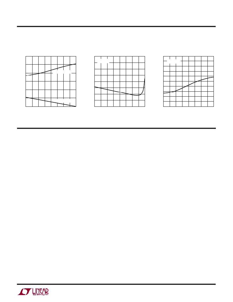
�2.2�
�V� C� Pin� Threshold� and� High�
�Clamp� Voltage� vs� Temperature�
�800�
�Feedback� Input� Current�
�vs� Temperature�
�0�
�Negative� Feedback� Input� Current�
�vs� Temperature�
�2.0�
�700�
�V� FB� =V� REF�
�–10�
�V� NFB� =V� NFR�
�600�
�1.8�
�1.6�
�1.4�
�1.2�
�V� C� HIGH CLAMP�
�V� C� THRESHOLD�
�500�
�400�
�300�
�200�
�100�
�–20�
�–30�
�–40�
�1.0�
�–50� –25�
�0�
�25�
�50�
�75�
�100� 125� 150�
�0�
�–50� –25�
�0�
�25�
�50�
�75�
�100� 125� 150�
�–50�
�–50� –25�
�0�
�25�
�50�
�75�
�100� 125� 150�
�TEMPERATURE� (� °� C)�
�PI� N� FU� N� CTIO� N� S�
�LT1370� ?� G10�
�TEMPERATURE� (� °� C)�
�LT1370� ?� G11�
�TEMPERATURE� (� °� C)�
�LT1370� ?� G12�
�V� C� :� The� Compensation� pin� is� used� for� frequency� compen-�
�sation,� current� limiting� and� soft� start.� It� is� the� output� of� the�
�error� amplifier� and� the� input� of� the� current� comparator.�
�Loop� frequency� compensation� can� be� performed� with� an�
�RC� network� connected� from� the� V� C� pin� to� ground.� See�
�Applications� Information.�
�FB:� The� Feedback� pin� is� used� for� positive� output� voltage�
�sensing� and� oscillator� frequency� shifting.� It� is� the� invert-�
�ing� input� to� the� error� amplifier.� The� noninverting� input� of�
�this� amplifier� is� internally� tied� to� a� 1.245V� reference.�
�NFB:� The� Negative� Feedback� pin� is� used� for� negative�
�output� voltage� sensing.� It� is� connected� to� the� inverting�
�input� of� the� negative� feedback� amplifier� through� a� 100k�
�source� resistor.�
�S/S:� Shutdown� and� Synchronization� Pin.� The� S/S� pin� is�
�logic� level� compatible.� Shutdown� is� active� low� and� the�
�shutdown� threshold� is� typically� 1.3V.� For� normal� opera-�
�tion,� pull� the� S/S� pin� high,� tie� it� to� V� IN� or� leave� it� floating.� To�
�synchronize� switching,� drive� the� S/S� pin� between� 600kHz�
�and� 800kHz.� See� Applications� Information.�
�V� IN� :� Bypass� Input� Supply� Pin� with� a� Low� ESR� Capacitor,�
�10� μ� F� or� More.� The� regulator� goes� into� undervoltage� lock-�
�out� when� V� IN� drops� below� 2.5V.� Undervoltage� lockout�
�stops� switching� and� pulls� the� V� C� pin� low.�
�V� SW� :� The� Switch� pin� is� the� collector� of� the� power� switch�
�and� has� large� currents� flowing� through� it.� Keep� the� traces�
�to� the� switching� components� as� short� as� possible� to�
�minimize� radiation� and� voltage� spikes.�
�GND:� Tie� all� ground� pins� to� a� good� quality� ground� plane.�
�See� Applications� Information.�
�sn1370� 1370fs�
�5�
�相关PDF资料 |
PDF描述 |
|---|---|
| EBA36DTKD | CONN EDGECARD 72POS DIP .125 SLD |
| LT1082IQ#PBF | IC REG MULTI CONFIG 1A D2PAK |
| PM1812-6R8J | INDUCTOR 6.8UH 5% 1812 SMD |
| TVX1J102MCD | CAP ALUM 1000UF 63V 20% AXIAL |
| VE-2WY-EY-F1 | CONVERTER MOD DC/DC 3.3V 33W |
相关代理商/技术参数 |
参数描述 |
|---|---|
| LT1370CRTRPBF | 制造商:Linear Technology 功能描述: |
| LT1370CT7 | 功能描述:IC REG MULTI CONFIG ADJ TO220-7 RoHS:否 类别:集成电路 (IC) >> PMIC - 稳压器 - DC DC 开关稳压器 系列:- 设计资源:Design Support Tool 标准包装:1 系列:- 类型:升压(升压) 输出类型:固定 输出数:1 输出电压:3V 输入电压:0.75 V ~ 2 V PWM 型:- 频率 - 开关:- 电流 - 输出:100mA 同步整流器:是 工作温度:-40°C ~ 85°C 安装类型:表面贴装 封装/外壳:SOT-23-5 细型,TSOT-23-5 包装:剪切带 (CT) 供应商设备封装:TSOT-23-5 其它名称:AS1323-BTTT-30CT |
| LT1370CT7#PBF | 功能描述:IC REG MULTI CONFIG ADJ TO220-7 RoHS:是 类别:集成电路 (IC) >> PMIC - 稳压器 - DC DC 开关稳压器 系列:- 设计资源:Design Support Tool 标准包装:1 系列:- 类型:升压(升压) 输出类型:固定 输出数:1 输出电压:3V 输入电压:0.75 V ~ 2 V PWM 型:- 频率 - 开关:- 电流 - 输出:100mA 同步整流器:是 工作温度:-40°C ~ 85°C 安装类型:表面贴装 封装/外壳:SOT-23-5 细型,TSOT-23-5 包装:剪切带 (CT) 供应商设备封装:TSOT-23-5 其它名称:AS1323-BTTT-30CT |
| LT1370HV | 制造商:LINER 制造商全称:Linear Technology 功能描述:500kHz High Efficiency 6A Switching Regulator |
| LT1370HVCR | 功能描述:IC REG MULTI CONFIG ADJ 6A D2PAK RoHS:否 类别:集成电路 (IC) >> PMIC - 稳压器 - DC DC 开关稳压器 系列:- 设计资源:Design Support Tool 标准包装:1 系列:- 类型:升压(升压) 输出类型:固定 输出数:1 输出电压:3V 输入电压:0.75 V ~ 2 V PWM 型:- 频率 - 开关:- 电流 - 输出:100mA 同步整流器:是 工作温度:-40°C ~ 85°C 安装类型:表面贴装 封装/外壳:SOT-23-5 细型,TSOT-23-5 包装:剪切带 (CT) 供应商设备封装:TSOT-23-5 其它名称:AS1323-BTTT-30CT |
发布紧急采购,3分钟左右您将得到回复。