- 您现在的位置:买卖IC网 > PDF目录13833 > LT1370HVCT7 (Linear Technology)IC REG MULTI CONFIG ADJ TO220-7 PDF资料下载
参数资料
| 型号: | LT1370HVCT7 |
| 厂商: | Linear Technology |
| 文件页数: | 7/16页 |
| 文件大小: | 0K |
| 描述: | IC REG MULTI CONFIG ADJ TO220-7 |
| 标准包装: | 50 |
| 类型: | 降压(降压),升压(升压),反相,Cuk,回扫,正向转换器 |
| 输出类型: | 可调式 |
| 输出数: | 1 |
| 输出电压: | 1.25 V ~ 42 V |
| 输入电压: | 2.7 V ~ 25 V |
| PWM 型: | 电流模式 |
| 频率 - 开关: | 500kHz |
| 电流 - 输出: | 6A |
| 同步整流器: | 无 |
| 工作温度: | 0°C ~ 70°C |
| 安装类型: | 通孔 |
| 封装/外壳: | TO-220-7 成形引线 |
| 包装: | 管件 |
| 供应商设备封装: | TO-220-7 |
�� �
�
�LT1370�
�OPERATIO� N�
�Unique� error� amplifier� circuitry� allows� the� LT1370� to�
�directly� regulate� negative� output� voltages.� The� negative�
�feedback� amplifier’s� 100k� source� resistor� is� brought� out�
�for� negative� output� voltage� sensing.� The� NFB� pin� regulates�
�at� –� 2.48V� while� the� amplifier� output� internally� drives� the�
�FB� pin� to� 1.245V.� This� architecture,� which� uses� the� same�
�main� error� amplifier,� prevents� duplicating� functions� and�
�maintains� ease� of� use.� Consult� LTC� Marketing� for� units�
�that� can� regulate� down� to� –� 1.25V.�
�The� error� signal� developed� at� the� amplifier� output� is�
�brought� out� externally.� This� pin� (V� C� )� has� three� different�
�APPLICATIO� S� I� FOR� ATIO�
�Positive� Output� Voltage� Setting�
�functions.� It� is� used� for� frequency� compensation,� current�
�limit� adjustment� and� soft� starting.� During� normal� regula-�
�tor� operation� this� pin� sits� at� a� voltage� between� 1V� (low�
�output� current)� and� 1.9V� (high� output� current).� The� error�
�amplifier� is� a� current� output� (g� m� )� type,� so� this� voltage� can�
�be� externally� clamped� for� lowering� current� limit.� Like-�
�wise,� a� capacitor� coupled� external� clamp� will� provide� soft�
�start.� Switch� duty� cycle� goes� to� zero� if� the� V� C� pin� is� pulled�
�below� the� control� pin� threshold,� placing� the� LT1370� in� an�
�idle� mode.�
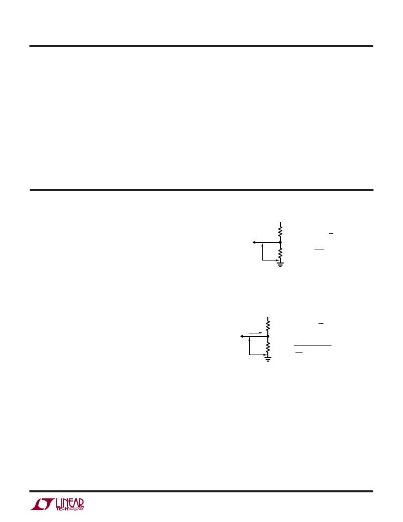
�V� OUT�
�(� )�
�V� OUT� =� V� REF� 1� +� R1�
�(� )�
�V� OUT�
�TheLT1370developsa1.245Vreference(V� REF� )fromthe�
�FB� pin� to� ground.� Output� voltage� is� set� by� connecting� the�
�FB� pin� to� an� output� resistor� divider� (Figure� 1).� The� FB� pin�
�bias� current� represents� a� small� error� and� can� usually� be�
�FB�
�PIN�
�V� REF�
�R1�
�R2�
�R1� =� R2� –1�
�R2�
�1.245�
�LT1370� ?� F01�
�ignored� for� values� of� R2� up� to� 7k.� The� suggested� value� for�
�R2� is� 6.19k.� The� NFB� pin� is� normally� left� open� for� positive�
�output� applications.� Positive� fixed� voltage� versions� are�
�available� (consult� LTC� Marketing).�
�Figure� 1.� Positive� Output� Resistor� Divider�
�(� )�
�–V� OUT� =� V� NFB� 1� +� R1� +� I� NFB� (R1)�
�?� V� OUT� ?� –� 2.48�
�(� )(� )�
�Negative Output Voltage Setting�
�The� LT1370� develops� a� –� 2.48V� reference� (V� NFR� )� from� the�
�NFB� pin� to� ground.� Output� voltage� is� set� by� connecting� the�
�NFB� pin� to� an� output� resistor� divider� (Figure� 2).� The�
�–30� μ� A� NFB� pin� bias� current� (I� NFB� )� can� cause� output�
�voltage� errors� and� should� not� be� ignored.� This� has� been�
�NFB�
�PIN�
�V� NFR�
�I� NFB�
�–V� OUT�
�R1�
�R2�
�R1� =�
�R2�
�2.48� +� 30� ?� 10� –� 6�
�R2�
�LT1370� ?� F02�
�accounted� for� in� the� formula� in� Figure� 2.� The� suggested�
�value� for� R2� is� 2.49k.� The� FB� pin� is� normally� left� open� for�
�negative� output� applications.�
�Dual� Polarity� Output� Voltage� Sensing�
�Certain� applications� benefit� from� sensing� both� positive�
�and� negative� output� voltages.� One� example� is� the� “Dual�
�Output� Flyback� Converter� with� Overvoltage� Protection”�
�circuit� shown� in� the� Typical� Applications� section.� Each�
�output� voltage� resistor� divider� is� individually� set� as�
�described� above.� When� both� the� FB� and� NFB� pins� are� used,�
�Figure� 2.� Negative� Output� Resistor� Divider�
�the� LT1370� acts� to� prevent� either� output� from� going�
�beyond� its� set� output� voltage.� For� example,� in� this� applica-�
�tion� if� the� positive� output� were� more� heavily� loaded� than�
�the� negative,� the� negative� output� would� be� greater� and�
�would� regulate� at� the� desired� set-point� voltage.� The� posi-�
�tive� output� would� sag� slightly� below� its� set-point� voltage.�
�This� technique� prevents� either� output� from� going� unregu-�
�lated� high� at� no� load.�
�sn1370� 1370fs�
�7�
�相关PDF资料 |
PDF描述 |
|---|---|
| LT1074IT | IC REG MULTI CONFIG ADJ TO220-5 |
| L04026R8BHLTR | INDUCTOR THIN FILM 6.8NH 0402 |
| L04025R6BHLTR | INDUCTOR THIN FILM 5.6NH 0402 |
| LT1076HVCT7-5 | IC REG MULTI CONFIG 5V TO220-7 |
| LT1076HVCT7#PBF | IC REG MULTI CONFIG ADJ TO220-7 |
相关代理商/技术参数 |
参数描述 |
|---|---|
| LT1370HVCT7#PBF | 功能描述:IC REG MULTI CONFIG ADJ TO220-7 RoHS:是 类别:集成电路 (IC) >> PMIC - 稳压器 - DC DC 开关稳压器 系列:- 产品培训模块:MIC23xxx HyperLight Load™ Regulators 标准包装:5,000 系列:HyperLight Load® 类型:降压(降压) 输出类型:固定 输出数:1 输出电压:1.8V 输入电压:2.7 V ~ 5.5 V PWM 型:混合物 频率 - 开关:4MHz 电流 - 输出:2A 同步整流器:是 工作温度:-40°C ~ 125°C 安装类型:表面贴装 封装/外壳:8-VFDFN 裸露焊盘,8-MLF? 包装:带卷 (TR) 供应商设备封装:8-MLF?(2x2) 产品目录页面:1094 (CN2011-ZH PDF) 其它名称:576-3303-2 |
| LT1370HVIR | 功能描述:IC REG MULTI CONFIG ADJ 6A D2PAK RoHS:否 类别:集成电路 (IC) >> PMIC - 稳压器 - DC DC 开关稳压器 系列:- 设计资源:Design Support Tool 标准包装:1 系列:- 类型:升压(升压) 输出类型:固定 输出数:1 输出电压:3V 输入电压:0.75 V ~ 2 V PWM 型:- 频率 - 开关:- 电流 - 输出:100mA 同步整流器:是 工作温度:-40°C ~ 85°C 安装类型:表面贴装 封装/外壳:SOT-23-5 细型,TSOT-23-5 包装:剪切带 (CT) 供应商设备封装:TSOT-23-5 其它名称:AS1323-BTTT-30CT |
| LT1370HVIR#PBF | 功能描述:IC REG MULTI CONFIG ADJ 6A D2PAK RoHS:是 类别:集成电路 (IC) >> PMIC - 稳压器 - DC DC 开关稳压器 系列:- 标准包装:250 系列:- 类型:降压(降压) 输出类型:固定 输出数:1 输出电压:1.2V 输入电压:2.05 V ~ 6 V PWM 型:电压模式 频率 - 开关:2MHz 电流 - 输出:500mA 同步整流器:是 工作温度:-40°C ~ 85°C 安装类型:表面贴装 封装/外壳:6-UFDFN 包装:带卷 (TR) 供应商设备封装:6-SON(1.45x1) 产品目录页面:1032 (CN2011-ZH PDF) 其它名称:296-25628-2 |
| LT1370HVIR#TR | 功能描述:IC REG MULTI CONFIG ADJ 6A D2PAK RoHS:否 类别:集成电路 (IC) >> PMIC - 稳压器 - DC DC 开关稳压器 系列:- 设计资源:Design Support Tool 标准包装:1 系列:- 类型:升压(升压) 输出类型:固定 输出数:1 输出电压:3V 输入电压:0.75 V ~ 2 V PWM 型:- 频率 - 开关:- 电流 - 输出:100mA 同步整流器:是 工作温度:-40°C ~ 85°C 安装类型:表面贴装 封装/外壳:SOT-23-5 细型,TSOT-23-5 包装:剪切带 (CT) 供应商设备封装:TSOT-23-5 其它名称:AS1323-BTTT-30CT |
| LT1370HVIR#TRPBF | 功能描述:IC REG MULTI CONFIG ADJ 6A D2PAK RoHS:是 类别:集成电路 (IC) >> PMIC - 稳压器 - DC DC 开关稳压器 系列:- 设计资源:Design Support Tool 标准包装:1 系列:- 类型:升压(升压) 输出类型:固定 输出数:1 输出电压:3V 输入电压:0.75 V ~ 2 V PWM 型:- 频率 - 开关:- 电流 - 输出:100mA 同步整流器:是 工作温度:-40°C ~ 85°C 安装类型:表面贴装 封装/外壳:SOT-23-5 细型,TSOT-23-5 包装:剪切带 (CT) 供应商设备封装:TSOT-23-5 其它名称:AS1323-BTTT-30CT |
发布紧急采购,3分钟左右您将得到回复。