- 您现在的位置:买卖IC网 > PDF目录13973 > LT1372CS8#TR (Linear Technology)IC REG MULTI CONFIG ADJ 8SOIC PDF资料下载
参数资料
| 型号: | LT1372CS8#TR |
| 厂商: | Linear Technology |
| 文件页数: | 6/12页 |
| 文件大小: | 0K |
| 描述: | IC REG MULTI CONFIG ADJ 8SOIC |
| 标准包装: | 2,500 |
| 类型: | 降压(降压),升压(升压),反相,Cuk,回扫,正向转换器 |
| 输出类型: | 可调式 |
| 输出数: | 1 |
| 输出电压: | 1.25 V ~ 30 V |
| 输入电压: | 2.7 V ~ 25 V |
| PWM 型: | 电流模式 |
| 频率 - 开关: | 500kHz |
| 电流 - 输出: | 1.5A |
| 同步整流器: | 无 |
| 工作温度: | 0°C ~ 125°C |
| 安装类型: | 表面贴装 |
| 封装/外壳: | 8-SOIC(0.154",3.90mm 宽) |
| 包装: | 带卷 (TR) |
| 供应商设备封装: | 8-SOIC |
�� �
�
�LT1372/LT1377�
�OPERATIO�
�The� LT1372/LT1377� are� current� mode� switchers.� This�
�means� that� switch� duty� cycle� is� directly� controlled� by�
�switch� current� rather� than� by� output� voltage.� Referring� to�
�the� block� diagram,� the� switch� is� turned� “On”� at� the� start� of�
�each� oscillator� cycle.� It� is� turned� “Off”� when� switch� current�
�reaches� a� predetermined� level.� Control� of� output� voltage� is�
�obtained� by� using� the� output� of� a� voltage� sensing� error�
�amplifier� to� set� current� trip� level.� This� technique� has�
�several� advantages.� First,� it� has� immediate� response� to�
�input� voltage� variations,� unlike� voltage� mode� switchers�
�which� have� notoriously� poor� line� transient� response.�
�Second,� it� reduces� the� 90� °� phase� shift� at� mid-frequencies�
�in� the� energy� storage� inductor.� This� greatly� simplifies�
�closed-loop� frequency� compensation� under� widely� vary-�
�ing� input� voltage� or� output� load� conditions.� Finally,� it�
�allows� simple� pulse-by-pulse� current� limiting� to� provide�
�maximum� switch� protection� under� output� overload� or�
�short� conditions.� A� low� dropout� internal� regulator� pro-�
�vides� a� 2.3V� supply� for� all� internal� circuitry.� This� low�
�dropout� design� allows� input� voltage� to� vary� from� 2.7V� to�
�25V� with� virtually� no� change� in� device� performance.� A�
�500kHz� (LT1372)� or� 1MHz� (LT1377)� oscillator� is� the� basic�
�clock� for� all� internal� timing.� It� turns� “On”� the� output� switch�
�via� the� logic� and� driver� circuitry.� Special� adaptive� anti-sat�
�circuitry� detects� onset� of� saturation� in� the� power� switch�
�and� adjusts� driver� current� instantaneously� to� limit� switch�
�saturation.� This� minimizes� driver� dissipation� and� provides�
�very� rapid� turn-off� of� the� switch.�
�A� 1.245V� bandgap� reference� biases� the� positive� input� of�
�the� error� amplifier.� The� negative� input� of� the� amplifier� is�
�brought� out� for� positive� output� voltage� sensing.� The� error�
�amplifier� has� nonlinear� transconductance� to� reduce� out-�
�APPLICATIO� S� I� FOR� ATIO�
�Positive� Output� Voltage� Setting�
�put� overshoot� on� start-up� or� overload� recovery.� When�
�the� feedback� voltage� exceeds� the� reference� by� 40mV,�
�error� amplifier� transconductance� increases� ten� times,�
�which� reduces� output� overshoot.� The� feedback� input� also�
�invokes� oscillator� frequency� shifting,� which� helps� pro-�
�tect� components� during� overload� conditions.� When� the�
�feedback� voltage� drops� below� 0.6V,� the� oscillator� fre-�
�quency� is� reduced� 5:1.� Lower� switching� frequency� allows�
�full� control� of� switch� current� limit� by� reducing� minimum�
�switch� duty� cycle.�
�Unique� error� amplifier� circuitry� allows� the� LT1372/LT1377�
�to� directly� regulate� negative� output� voltages.� The� negative�
�feedback� amplifier’s� 100k� source� resistor� is� brought� out�
�for� negative� output� voltage� sensing.� The� NFB� pin� regulates�
�at� –� 2.49V� while� the� amplifier� output� internally� drives� the�
�FB� pin� to� 1.245V.� This� architecture,� which� uses� the� same�
�main� error� amplifier,� prevents� duplicating� functions� and�
�maintains� ease� of� use.� Consult� Linear� Technology� Market-�
�ing� for� units� that� can� regulate� down� to� –� 1.25V.�
�The� error� signal� developed� at� the� amplifier� output� is�
�brought� out� externally.� This� pin� (V� C� )� has� three� different�
�functions.� It� is� used� for� frequency� compensation,� current�
�limit� adjustment� and� soft� starting.� During� normal� regula-�
�tor� operation� this� pin� sits� at� a� voltage� between� 1V� (low�
�output� current)� and� 1.9V� (high� output� current).� The� error�
�amplifier� is� a� current� output� (g� m� )� type,� so� this� voltage� can�
�be� externally� clamped� for� lowering� current� limit.� Like-�
�wise,� a� capacitor� coupled� external� clamp� will� provide� soft�
�start.� Switch� duty� cycle� goes� to� zero� if� the� V� C� pin� is� pulled�
�below� the� control� pin� threshold,� placing� the� LT1372/�
�LT1377� in� an� idle� mode.�
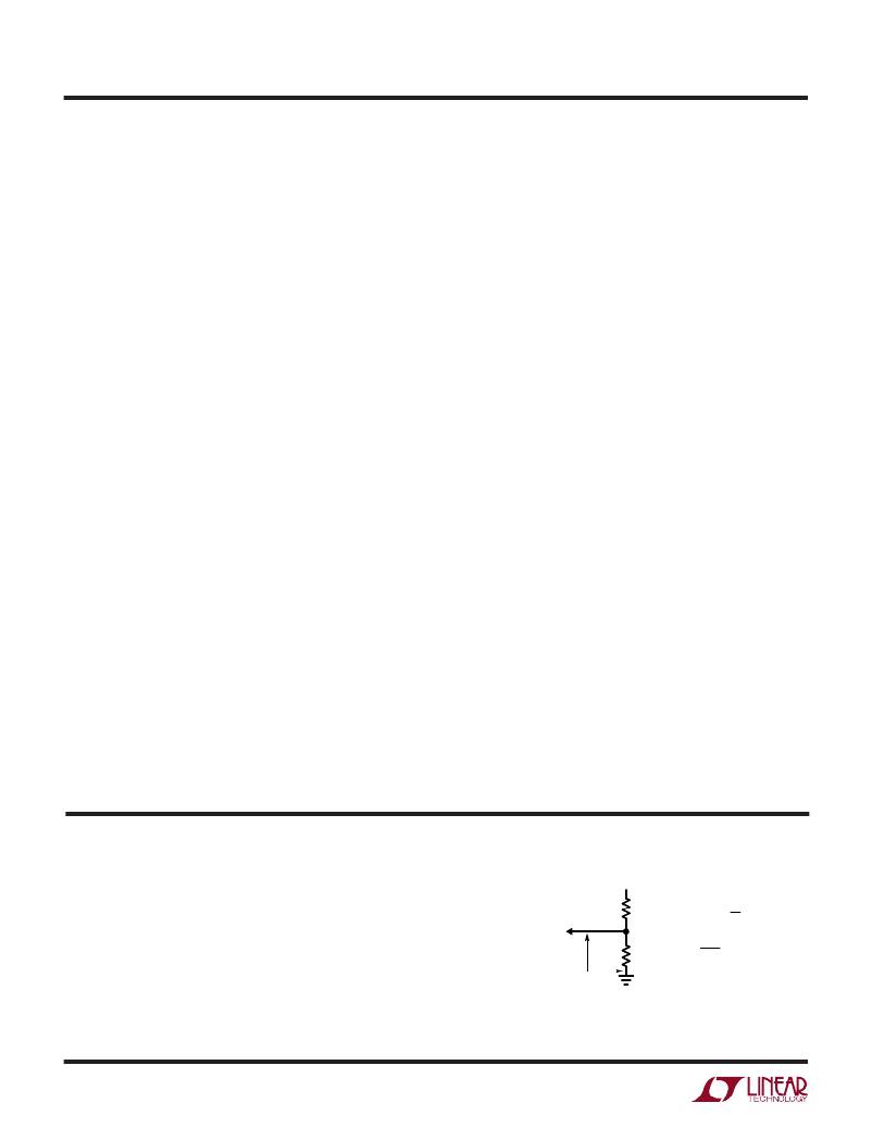
�V� OUT�
�(� )�
�V� OUT� =� V� REF� 1� +� R1�
�(� )�
�V� OUT�
�TheLT1372/LT1377developsa1.245Vreference(V� REF� )�
�from� the� FB� pin� to� ground.� Output� voltage� is� set� by�
�connecting� the� FB� pin� to� an� output� resistor� divider�
�(Figure� 1).� The� FB� pin� bias� current� represents� a� small�
�FB�
�PIN�
�V� REF�
�R1�
�R2�
�R1� =� R2� –1�
�1.245�
�R2�
�error� and� can� usually� be� ignored� for� values� of� R2� up� to� 7k.�
�The� suggested� value� for� R2� is� 6.19k.� The� NFB� pin� is�
�normally� left� open� for� positive� output� applications.�
�6�
�LT1372� ?� F01�
�Figure� 1.� Positive� Output� Resistor� Divider�
�相关PDF资料 |
PDF描述 |
|---|---|
| LT1507CS8#TRPBF | IC REG BUCK ADJ 1.5A 8SOIC |
| DS1232S+T&R | IC MICRO MONITOR 16-SOIC |
| 10MH747MEFCT56.3X7 | CAP ALUM 47UF 10V 20% RADIAL |
| 10MH747MEFCTZ6.3X7 | CAP ALUM 47UF 10V 20% RADIAL |
| GEM15DTBD-S273 | CONN EDGECARD 30POS R/A .156 SLD |
相关代理商/技术参数 |
参数描述 |
|---|---|
| LT1372HV | 制造商:LINER 制造商全称:Linear Technology 功能描述:500kHz and 1MHz High Efficiency 1.5A Switching Regulators |
| LT1372HVCN8 | 功能描述:IC REG MULTI CONFIG ADJ 8DIP RoHS:否 类别:集成电路 (IC) >> PMIC - 稳压器 - DC DC 开关稳压器 系列:- 标准包装:2,500 系列:- 类型:降压(降压) 输出类型:固定 输出数:1 输出电压:1.2V,1.5V,1.8V,2.5V 输入电压:2.7 V ~ 20 V PWM 型:- 频率 - 开关:- 电流 - 输出:50mA 同步整流器:是 工作温度:-40°C ~ 125°C 安装类型:表面贴装 封装/外壳:10-TFSOP,10-MSOP(0.118",3.00mm 宽)裸露焊盘 包装:带卷 (TR) 供应商设备封装:10-MSOP 裸露焊盘 |
| LT1372HVCN8#PBF | 功能描述:IC REG MULTI CONFIG ADJ 8DIP RoHS:是 类别:集成电路 (IC) >> PMIC - 稳压器 - DC DC 开关稳压器 系列:- 标准包装:20 系列:SIMPLE SWITCHER® 类型:降压(降压) 输出类型:固定 输出数:1 输出电压:12V 输入电压:4 V ~ 60 V PWM 型:电压模式 频率 - 开关:52kHz 电流 - 输出:1A 同步整流器:无 工作温度:-40°C ~ 125°C 安装类型:通孔 封装/外壳:16-DIP(0.300",7.62mm) 包装:管件 供应商设备封装:16-DIP 其它名称:*LM2575HVN-12LM2575HVN-12 |
| LT1372HVCS8 | 功能描述:IC REG MULTI CONFIG ADJ 8SOIC RoHS:否 类别:集成电路 (IC) >> PMIC - 稳压器 - DC DC 开关稳压器 系列:- 标准包装:2,500 系列:- 类型:降压(降压) 输出类型:固定 输出数:1 输出电压:1.2V,1.5V,1.8V,2.5V 输入电压:2.7 V ~ 20 V PWM 型:- 频率 - 开关:- 电流 - 输出:50mA 同步整流器:是 工作温度:-40°C ~ 125°C 安装类型:表面贴装 封装/外壳:10-TFSOP,10-MSOP(0.118",3.00mm 宽)裸露焊盘 包装:带卷 (TR) 供应商设备封装:10-MSOP 裸露焊盘 |
| LT1372HVCS8#PBF | 功能描述:IC REG MULTI CONFIG ADJ 8SOIC RoHS:是 类别:集成电路 (IC) >> PMIC - 稳压器 - DC DC 开关稳压器 系列:- 标准包装:250 系列:- 类型:降压(降压) 输出类型:固定 输出数:1 输出电压:1.2V 输入电压:2.05 V ~ 6 V PWM 型:电压模式 频率 - 开关:2MHz 电流 - 输出:500mA 同步整流器:是 工作温度:-40°C ~ 85°C 安装类型:表面贴装 封装/外壳:6-UFDFN 包装:带卷 (TR) 供应商设备封装:6-SON(1.45x1) 产品目录页面:1032 (CN2011-ZH PDF) 其它名称:296-25628-2 |
发布紧急采购,3分钟左右您将得到回复。