- 您现在的位置:买卖IC网 > PDF目录14798 > LT1372IS8#PBF (Linear Technology)IC REG MULTI CONFIG ADJ 8SOIC PDF资料下载
参数资料
| 型号: | LT1372IS8#PBF |
| 厂商: | Linear Technology |
| 文件页数: | 7/12页 |
| 文件大小: | 0K |
| 描述: | IC REG MULTI CONFIG ADJ 8SOIC |
| 标准包装: | 100 |
| 类型: | 降压(降压),升压(升压),反相,Cuk,回扫,正向转换器 |
| 输出类型: | 可调式 |
| 输出数: | 1 |
| 输出电压: | 1.25 V ~ 30 V |
| 输入电压: | 2.7 V ~ 25 V |
| PWM 型: | 电流模式 |
| 频率 - 开关: | 500kHz |
| 电流 - 输出: | 1.5A |
| 同步整流器: | 无 |
| 工作温度: | -40°C ~ 125°C |
| 安装类型: | 表面贴装 |
| 封装/外壳: | 8-SOIC(0.154",3.90mm 宽) |
| 包装: | 管件 |
| 供应商设备封装: | 8-SOIC |
| 产品目录页面: | 1327 (CN2011-ZH PDF) |
�� �
�
�LT1372/LT1377�
�APPLICATIO� S� I� FOR� ATIO�
�Positive� fixed� voltage� versions� are� available� (consult�
�Linear� Technology� marketing).�
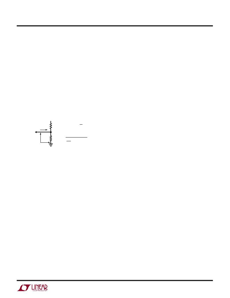
�Negative� Output� Voltage� Setting�
�The� LT1372/LT1377� develops� a� –� 2.49V� reference� (V� NFR� )�
�from� the� NFB� pin� to� ground.� Output� voltage� is� set� by�
�connecting� the� NFB� pin� to� an� output� resistor� divider�
�(Figure� 2).� The� –� 30� μ� A� NFB� pin� bias� current� (I� NFB� )� can�
�cause� output� voltage� errors� and� should� not� be� ignored.�
�This� has� been� accounted� for� in� the� formula� in� Figure� 2.� The�
�suggested� value� for� R2� is� 2.49k.� The� FB� pin� is� normally� left�
�open� for� negative� output� application.� See� Dual� Polarity�
�Output� Voltage� Sensing� for� limitatins� on� FB� pin� loading�
�when� using� the� NFB� pin.�
�Shutdown� and� Synchronization�
�The� dual� function� S/S� pin� provides� easy� shutdown� and�
�synchronization.� It� is� logic� level� compatible� and� can� be�
�pulled� high,� tied� to� V� IN� or� left� floating� for� normal� operation.�
�A� logic� low� on� the� S/S� pin� activates� shutdown,� reducing�
�the� part’s� supply� current� to� 12� μ� A.� Typical� synchronization�
�range� is� from� 1.05� to� 1.8� times� the� part’s� natural� switching�
�frequency,� but� is� only� guaranteed� between� 600kHz� and�
�800kHz� (LT1372)� or� 1.2MHz� and� 1.6MHz� (LT1377).� At�
�start-up,� the� synchronization� signal� should� not� be� applied�
�until� the� feedback� pin� is� above� the� frequency� shift� voltage�
�of� 0.7V.� If� the� NFB� pin� is� used,� synchronization� should� not�
�be� applied� until� the� NFB� pin� is� more� negative� than� –� 1.4V.�
�A� 12� μ� s� resetable� shutdown� delay� network� guarantees� the�
�(� )�
�–V� OUT� =� V� NFB� 1� +� R1� +� I� NFB� (R1)�
�I� NFB�
�–V� OUT�
�R1�
�R2�
�part� will� not� go� into� shutdown� while� receiving� a� synchro-�
�nization� signal.�
�(� )(�
�NFB�
�PIN�
�V� NFR�
�R2�
�R1� =�
�?� V� OUT� ?� –� 2.49�
�2.49� +� 30� ×� 10� –6�
�R2�
�)�
�LT1372� ?� F02�
�Caution� should� be� used� when� synchronizing� above� 700kHz�
�(LT1372)� or� 1.4MHz� (LT1377)� because� at� higher� sync�
�frequencies� the� amplitude� of� the� internal� slope� compensa-�
�tion� used� to� prevent� subharmonic� switching� is� reduced.�
�Figure� 2.� Negative� Output� Resistor� Divider�
�Dual� Polarity� Output� Voltage� Sensing�
�Certain� applications� benefit� from� sensing� both� positive�
�and� negative� output� voltages.� One� example� is� the� “Dual�
�Output� Flyback� Converter� with� Overvoltage� Protection”�
�circuit� shown� in� the� Typical� Applications� section.� Each�
�output� voltage� resistor� divider� is� individually� set� as� de-�
�scribed� above.� When� both� the� FB� and� NFB� pins� are� used,�
�the� LT1372/LT1377� acts� to� prevent� either� output� from�
�going� beyond� its� set� output� voltage.� For� example� in� this�
�application,� if� the� positive� output� were� more� heavily� loaded�
�than� the� negative,� the� negative� output� would� be� greater�
�and� would� regulate� at� the� desired� set-point� voltage.� The�
�positive� output� would� sag� slightly� below� its� set-point�
�voltage.� This� technique� prevents� either� output� from� going�
�unregulated� high� at� no� load.� Please� note� that� the� load� on�
�the� FB� pin� should� not� exceed� 250� μ� A� when� the� NFB� pin� is�
�used.� This� situation� occurs� when� the� resistor� dividers� are�
�used� at� both� FB� and� NFB.� True� load� on� FB� is� not� the� full�
�divider� current� unless� the� positive� output� is� shorted� to�
�ground.� See� Dual� Output� Flyback� Converter� application.�
�This� type� of� subharmonic� switching� only� occurs� when� the�
�duty� cycle� of� the� switch� is� above� 50%.� Higher� inductor�
�values� will� tend� to� eliminate� problems.�
�Thermal� Considerations�
�Care� should� be� taken� to� ensure� that� the� worst-case� input�
�voltage� and� load� current� conditions� do� not� cause� exces-�
�sive� die� temperatures.� The� packages� are� rated� at� 120� °� C/W�
�for� SO� (S8)� and� 130� °� C/W� for� PDIP� (N8).�
�Average� supply� current� (including� driver� current)� is:�
�I� IN� =� 4mA� +� DC� (I� SW� /60� +� I� SW� � 0.004)�
�I� SW� =� switch� current�
�DC� =� switch� duty� cycle�
�Switch� power� dissipation� is� given� by:�
�P� SW� =� (I� SW� )� 2� � R� SW� � DC�
�R� SW� =� output� switch� “On”� resistance�
�Total� power� dissipation� of� the� die� is� the� sum� of� supply�
�current� times� supply� voltage� plus� switch� power:�
�P� D(TOTAL)� =� (I� IN� � V� IN� )� +� P� SW�
�7�
�相关PDF资料 |
PDF描述 |
|---|---|
| ABC05DRYI-S13 | CONN EDGECARD 10POS .100 EXTEND |
| LT1071CT#06PBF | IC REG MULTI CONFIG ADJ TO220-5 |
| RBC25DRYI | CONN EDGECARD 50POS DIP .100 SLD |
| LT1376HVIS8#PBF | IC REG BUCK ADJ 1.5A 8SOIC |
| RCC25DRXI | CONN EDGECARD 50POS DIP .100 SLD |
相关代理商/技术参数 |
参数描述 |
|---|---|
| LT1373 | 制造商:LINER 制造商全称:Linear Technology 功能描述:250kHz Low Supply Current High Efficiency 1.5A Switching Regulator |
| LT13735IS8 | 制造商:Linear Technology 功能描述: |
| LT1373CN8 | 制造商:Linear Technology 功能描述:Conv DC-DC Single Non-Inv/Inv/Step Up/Step Down 2.7V to 25V 8-Pin PDIP N |
| LT1373CN8#PBF | 功能描述:IC REG MULTI CONFIG ADJ 8DIP RoHS:是 类别:集成电路 (IC) >> PMIC - 稳压器 - DC DC 开关稳压器 系列:- 标准包装:2,500 系列:- 类型:降压(降压) 输出类型:固定 输出数:1 输出电压:1.2V,1.5V,1.8V,2.5V 输入电压:2.7 V ~ 20 V PWM 型:- 频率 - 开关:- 电流 - 输出:50mA 同步整流器:是 工作温度:-40°C ~ 125°C 安装类型:表面贴装 封装/外壳:10-TFSOP,10-MSOP(0.118",3.00mm 宽)裸露焊盘 包装:带卷 (TR) 供应商设备封装:10-MSOP 裸露焊盘 |
| LT1373CN8PBF | 制造商:Linear Technology 功能描述:LT1373CN8PBF |
发布紧急采购,3分钟左右您将得到回复。