- 您现在的位置:买卖IC网 > PDF目录13998 > LT1373CN8#PBF (Linear Technology)IC REG MULTI CONFIG ADJ 8DIP PDF资料下载
参数资料
| 型号: | LT1373CN8#PBF |
| 厂商: | Linear Technology |
| 文件页数: | 5/12页 |
| 文件大小: | 0K |
| 描述: | IC REG MULTI CONFIG ADJ 8DIP |
| 标准包装: | 50 |
| 类型: | 降压(降压),升压(升压),反相,Cuk,回扫,正向转换器 |
| 输出类型: | 可调式 |
| 输出数: | 1 |
| 输出电压: | 1.25 V ~ 35 V |
| 输入电压: | 2.7 V ~ 25 V |
| PWM 型: | 电流模式 |
| 频率 - 开关: | 250kHz |
| 电流 - 输出: | 1.5A |
| 同步整流器: | 无 |
| 工作温度: | 0°C ~ 125°C |
| 安装类型: | 通孔 |
| 封装/外壳: | 8-DIP(0.300",7.62mm) |
| 包装: | 管件 |
| 供应商设备封装: | 8-PDIP |
| 产品目录页面: | 1327 (CN2011-ZH PDF) |
�� �
�
�LT1373�
�PI� FU� CTIO� S�
�V� C� (Pin� 1):� Compensation� Pin.� The� V� C� pin� is� used� for�
�frequency� compensation,� current� limiting� and� soft� start.� It�
�is� the� output� of� the� error� amplifier� and� the� input� of� the�
�current� comparator.� Loop� frequency� compensation� can� be�
�performed� with� an� RC� network� connected� from� the� V� C� pin�
�to� ground.�
�FB� (Pin� 2):� The� feedback� pin� is� used� for� positive� output�
�voltage� sensing� and� oscillator� frequency� shifting.� It� is� the�
�inverting� input� to� the� error� amplifier.� The� noninverting�
�input� of� this� amplifier� is� internally� tied� to� a� 1.245V�
�reference.� Load� on� the� FB� pin� should� not� exceed� 100� μ� A�
�when� the� NFB� pin� is� used.� See� Applications� Information.�
�NFB� (Pin� 3):� The� negative� feedback� pin� is� used� for� negative�
�output� voltage� sensing.� It� is� connected� to� the� inverting�
�input� of� the� negative� feedback� amplifier� through� a� 400k�
�source� resistor.�
�S/S� (Pin� 4):� Shutdown� and� Synchronization� Pin.� The� S/S�
�pin� is� logic� level� compatible.� Shutdown� is� active� low� and�
�the� shutdown� threshold� is� typically� 1.3V.� For� normal�
�operation,� pull� the� S/S� pin� high,� tie� it� to� V� IN� or� leave� it�
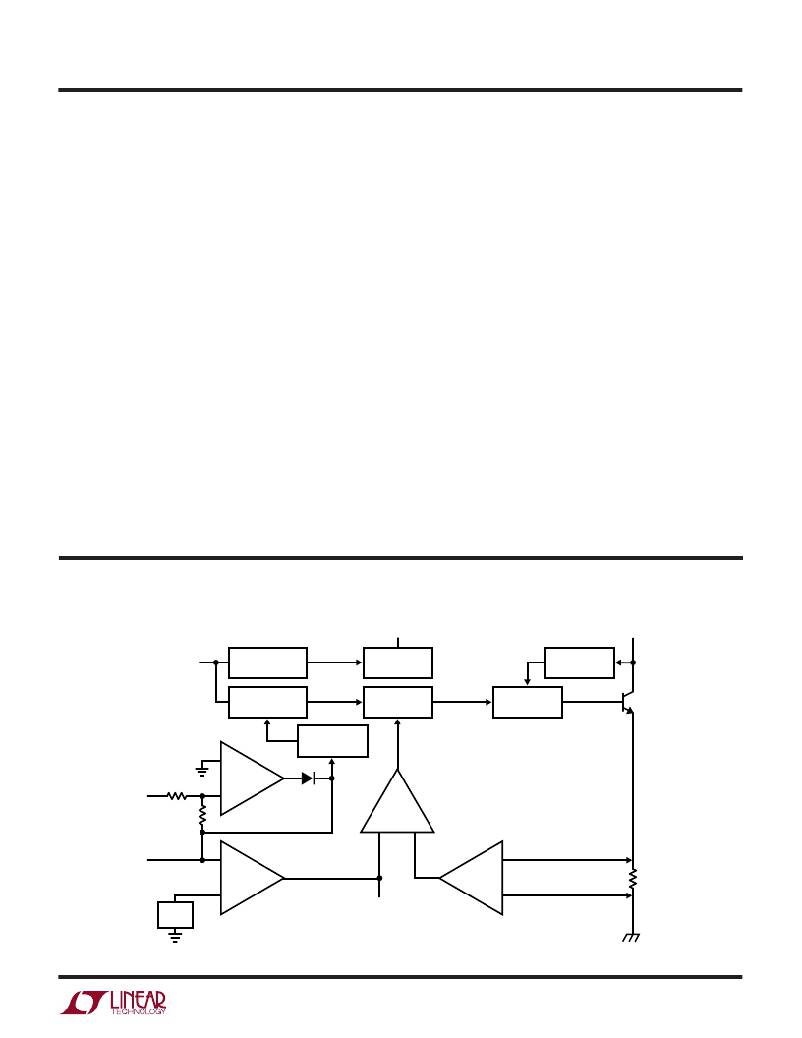
�BLOCK� DIAGRA�
�V� IN�
�floating.� To� synchronize� switching,� drive� the� S/S� pin� be-�
�tween� 300kHz� and� 340kHz.�
�V� IN� (Pin� 5):� Input� Supply� Pin.� Bypass� V� IN� with� 10� μ� F� or�
�more.� The� part� goes� into� undervoltage� lockout� when� V� IN�
�drops� below� 2.5V.� Undervoltage� lockout� stops� switching�
�and� pulls� the� V� C� pin� low.�
�GND� S� (Pin� 6):� The� ground� sense� pin� is� a� “clean”� ground.�
�The� internal� reference,� error� amplifier� and� negative� feed-�
�back� amplifier� are� referred� to� the� ground� sense� pin.� Con-�
�nect� it� to� ground.� Keep� the� ground� path� connection� to� the�
�output� resistor� divider� and� the� V� C� compensation� network�
�free� of� large� ground� currents.�
�GND� (Pin� 7):� The� ground� pin� is� the� emitter� connection� of�
�the� power� switch� and� has� large� currents� flowing� through� it.�
�It� should� be� connected� directly� to� a� good� quality� ground�
�plane.�
�V� SW� (Pin� 8):� The� switch� pin� is� the� collector� of� the� power�
�switch� and� has� large� currents� flowing� through� it.� Keep� the�
�traces� to� the� switching� components� as� short� as� possible� to�
�minimize� radiation� and� voltage� spikes.�
�SW�
�S/S�
�SHUTDOWN�
�DELAY� AND� RESET�
�LOW� DROPOUT�
�2.3V� REG�
�ANTI-SAT�
�SYNC�
�250kHz�
�OSC�
�LOGIC�
�DRIVER�
�SWITCH�
�5:1� FREQUENCY�
�SHIFT�
�+�
�NEGATIVE�
�–�
�NFB�
�400k�
�FEEDBACK�
�AMP�
�FB�
�200k�
�COMP�
�+�
�ERROR�
�AMP�
�CURRENT�
�AMP�
�0.08� ?�
�1.245V�
�V� C�
�A� V� ≈� 6�
�–�
�REF�
�GND� SENSE�
�GND�
�LT1373� ?� BD�
�5�
�相关PDF资料 |
PDF描述 |
|---|---|
| LTC1515CS8-3/5#PBF | IC REG MULTI CONFIG 3V/5V 8SOIC |
| LTC3545EUD-1#TRPBF | IC REG BUCK SYNC ADJ 0.8A 16QFN |
| 83823C | INDUCTOR 82.0UH 0.27A SMD |
| 16MS733MEFC6.3X7 | CAP ALUM 33UF 16V 20% RADIAL |
| MAX6865UK26D3S+T | IC MPU SUPERVISOR SOT23-5 |
相关代理商/技术参数 |
参数描述 |
|---|---|
| LT1373CS8 | 功能描述:IC REG MULTI CONFIG ADJ 8SOIC RoHS:否 类别:集成电路 (IC) >> PMIC - 稳压器 - DC DC 开关稳压器 系列:- 标准包装:2,500 系列:- 类型:降压(降压) 输出类型:固定 输出数:1 输出电压:1.2V,1.5V,1.8V,2.5V 输入电压:2.7 V ~ 20 V PWM 型:- 频率 - 开关:- 电流 - 输出:50mA 同步整流器:是 工作温度:-40°C ~ 125°C 安装类型:表面贴装 封装/外壳:10-TFSOP,10-MSOP(0.118",3.00mm 宽)裸露焊盘 包装:带卷 (TR) 供应商设备封装:10-MSOP 裸露焊盘 |
| LT1373CS8#/PBF | 制造商:Linear Technology 功能描述: |
| LT1373CS8#PBF | 功能描述:IC REG MULTI CONFIG ADJ 8SOIC RoHS:是 类别:集成电路 (IC) >> PMIC - 稳压器 - DC DC 开关稳压器 系列:- 标准包装:250 系列:- 类型:降压(降压) 输出类型:固定 输出数:1 输出电压:1.2V 输入电压:2.05 V ~ 6 V PWM 型:电压模式 频率 - 开关:2MHz 电流 - 输出:500mA 同步整流器:是 工作温度:-40°C ~ 85°C 安装类型:表面贴装 封装/外壳:6-UFDFN 包装:带卷 (TR) 供应商设备封装:6-SON(1.45x1) 产品目录页面:1032 (CN2011-ZH PDF) 其它名称:296-25628-2 |
| LT1373CS8#TR | 功能描述:IC REG MULTI CONFIG ADJ 8SOIC RoHS:否 类别:集成电路 (IC) >> PMIC - 稳压器 - DC DC 开关稳压器 系列:- 标准包装:2,500 系列:- 类型:降压(降压) 输出类型:固定 输出数:1 输出电压:1.2V,1.5V,1.8V,2.5V 输入电压:2.7 V ~ 20 V PWM 型:- 频率 - 开关:- 电流 - 输出:50mA 同步整流器:是 工作温度:-40°C ~ 125°C 安装类型:表面贴装 封装/外壳:10-TFSOP,10-MSOP(0.118",3.00mm 宽)裸露焊盘 包装:带卷 (TR) 供应商设备封装:10-MSOP 裸露焊盘 |
| LT1373CS8#TR/PBF | 制造商:Linear Technology 功能描述: |
发布紧急采购,3分钟左右您将得到回复。